
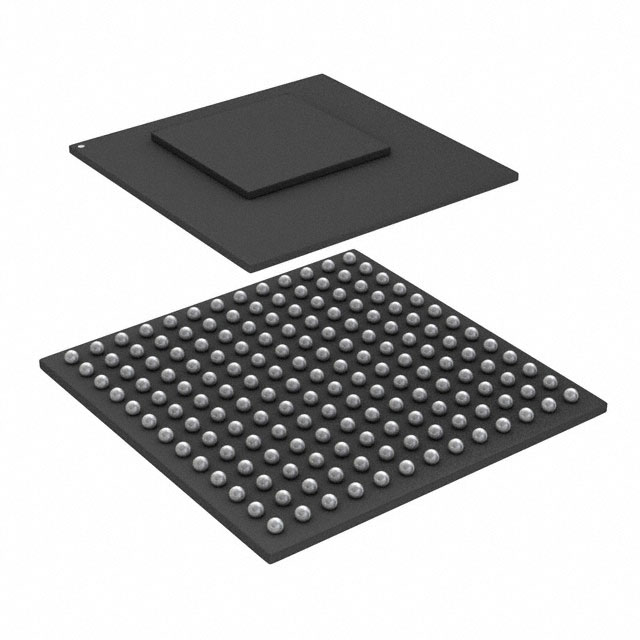
The AD91661is a high performance, wideband, on-chip vector signal generator composed of a high speed JESD204B serializer/deserializer (SERDES) interface, a flexible 16-bit digital datapath, a inphase/quadrature (I/Q) digital-to-analog converter (DAC) core, and an integrated differential to single-ended output buffer amplifier, matched to a 50 Ω load up to 10 GHz.The DAC core is based on a quad-switch architecture, which is configurable to increase the effective DAC core update rate of up to 12.8 GSPS from a 6.4 GHz DAC sampling clock, with an analog output bandwidth of true dc to 9.0 GHz, typically. The digital datapath includes multiple interpolation filter stages, a direct digital synthesizer (DDS) block with multiple numerically controlled oscillators (NCOs) supporting fast frequency hopping (FFH), and additional FIR85 and inverse sinc filter stages to allow flexible spectrum planning.The differential to single-ended buffer eliminates the need for a wideband balun, and supports the full analog output bandwidth of the DAC core. DC coupling the output allows baseband waveform generation without the need for external bias tees or similar circuitry, which makes the AD9166 uniquely suited for the most demanding high speed ultrawideband RF transmit applications.The various filter stages enable the AD9166 to be configured for lower data rates, while maintaining higher DAC clock rates to ease the filtering requirements and reduce the overall system size, weight, and power.The data interface receiver consists of up to eight JESD204B SERDES lanes, each capable of carrying up to 12.5 Gbps. To enable maximum flexibility, the receiver is fully configurable according to the data rate, number of SERDES lanes, and lane mapping required by the JESD204B transmitter.In 2× nonreturn-to-zero (NRZ) mode of operation (with FIR85 enabled), the AD9166 can reconstruct RF carriers from true dc to the edge of the third Nyquist zone, or an analog bandwidth of true dc up to 9 GHz.In mix mode, the AD9166 can reconstruct RF carriers in the second and third Nyquist zones while consuming lower power and maintaining a performance comparable to 2× NRZ mode.In baseband modes, such as return-to-zero (RZ) and 1× NRZ, the AD9166 is ideal to reconstruct RF carriers from true dc to the edge of the first Nyquist zone while consuming lower power compared to 2× NRZ mode.The quadrature DDS block can be configured as a digital upconverter to upconvert I/Q data samples to the desired location across the spectrum, in all three Nyquist zones.The DDS also consists of a bank of 32 numerically controlled oscillators (NCOs), each with its own 32-bit phase accumulator. When combined with a 100 MHz serial peripheral interface (SPI), the DDS allows a phase coherent FFH, with a phase settling time as low as 300 ns.The AD9166 is configured using a common SPI interface that monitors the status of all registers. The AD9166 is offered in a 324-ball, 15 mm × 15 mm, 0.8 mm pitch BGA_ED package.Product Highlights
YG GROUP (YUGUANG INTERNATIONAL(HK)CO.,LTD) supports reliable sourcing through quality controls and compliance documentation. Please confirm product requirements, applicable certifications and supporting documents before ordering.
AD9166 is an authentic electronic component manufactured by Analog Devices, categorized under Clock & Timer ICs. It is supplied in the standard manufacturer-specified package footprint, providing industry-standard mechanical dimensions and terminal configurations for board-level assembly. Full pinout configurations, physical footprint drawings, and rated operating tolerances are documented in the official AD9166 datasheet above.
Electronic component spot-market pricing for AD9166 fluctuates based on real-time global availability, production date codes, minimum order quantities (MOQ), and packaging formats (e.g., Reel, Tube, Tray). Using an RFQ ensures you receive accurate, real-time volume pricing tied to verified, traceable inventory rather than stale catalog estimates.
Lead times for AD9166 depend on whether stock is dispatched from our central hub or regional franchise partners. Ready-to-ship inventory typically leaves the warehouse within 1–3 business days following quality inspection, while factory-direct or back-ordered allocations are confirmed with an estimated ship date upon RFQ reply.
Loading articles…
Loading related products…
| Picture | Part Number | Manufacturer | PDF / RoHS | Stock | Action |
|---|---|---|---|---|---|
| Analog Devices | 6,470 | |||
| Analog Devices | 7,210 | |||
| Analog Devices | 7,900 | |||
 | Analog Devices | 9,380 | |||
| Analog Devices | 7,810 | |||
| Analog Devices | 3,430 | |||
 | Analog Devices | 3,640 | |||
 | Analog Devices | 9,070 | |||
 | Analog Devices | 9,150 | |||
 | Analog Devices | 6,550 |
Loading articles…
Explore MLCC miniaturization through Murata GRM158C80G226ME01D, linking its 22 µF, 4 V, 0402-inch specification to effective capacitance, consumer-use limits and real PCB area.
Read more →
Assess what the proposed Winbond–Infineon NOR Flash transaction means for W25Q64JVSSIQ sourcing, with dated deal status, exact-code checks and a practical alternative-qualification framework.
Read more →
Design an ALDP1F06 driver by checking its 6 V coil, diode-qualified release-time limit, flyback clamp stress, hot restart and the actual contact event required by the appliance.
Read more →
Use TAS5431QPWPRQ1 to assess an eCall speaker connection by interpreting load-test timing, I²C fault bits, open-load reporting and recovery during backup-supply transitions.
Read more →