
Eyki Chen




| Picture | Part Number | Manufacturer | Stock | Action |
|---|---|---|---|---|
 | GRM158C80G226ME01D | Murata | 6,060 |
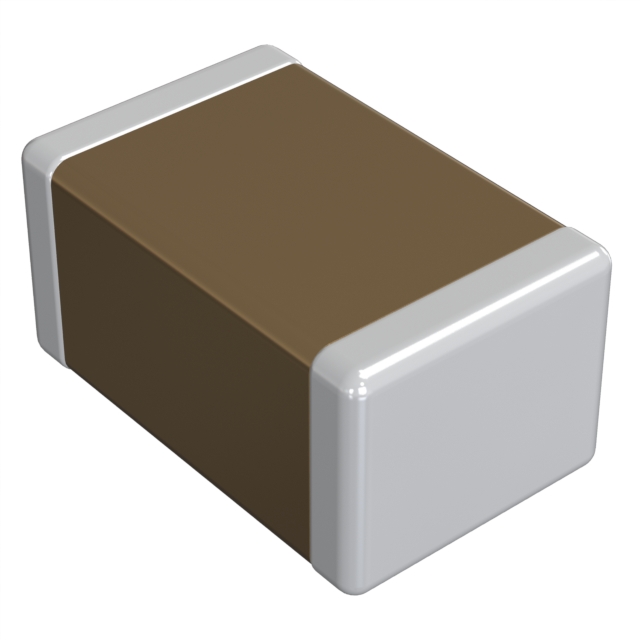
It is a Murata 22 µF, ±20%, 4 V X6S MLCC in a 0402-inch, or 1005-metric, body. The exact supplied rating table limits its application to consumer equipment. The D suffix identifies the specified paper-tape reel option.
No. The April 8, 2026 announcement concerns different GCM products with automotive qualification. It illustrates a broader density trend, but its qualification and performance claims do not transfer to this consumer GRM part.
No. The nominal value belongs to specified measurement conditions. Initial tolerance, DC bias, temperature and other influences must be addressed for the actual circuit. The supplied general example curves do not establish this exact part's biased capacitance.
One nominal 1.0 × 0.5 mm body has about 60.9% less plan-view area than a 1.6 × 0.8 mm body. That is a body-area calculation, not a PCB-footprint result. Required quantity, pads, spacing and routing determine the actual saving.
Category: Market&IndustryIntelligence
Author: Eyki Chen
GRM158C80G226ME01D illustrates how much nominal capacitance can fit into a small consumer-electronics component: 22 µF in a 0402-inch package, rated at 4 V with an X6S temperature characteristic. Its value to a crowded board depends on the capacitance retained in operation, the complete assembly footprint and the intended application. A smaller ceramic body creates an opportunity for higher density; the design earns that benefit only after electrical and manufacturing constraints have been checked.
On April 8, 2026, Murata announced mass production of seven automotive MLCCs aimed at increasing capacitance within constrained package sizes. The announcement includes low-voltage GCM parts and two 25 V devices. It describes a 100 µF product in 1206-inch size and a 1 µF, 25 V product in 0402-inch size, showing the same broad pressure to fit more capacitance around increasingly demanding electronics. These are different products from the GRM part examined here. Murata automotive MLCC announcement.
That distinction changes the selection decision. The supplied GRM158C80G226ME01 specification begins with broad family-level application language, but its exact rating table restricts the part to consumer equipment. The specific restriction governs this article. Neither the automotive qualification of the announced GCM products nor a broad statement about MLCC market demand establishes an automotive or industrial qualification for GRM158C80G226ME01D.
No. The short, current-limited proof test is an acceptance condition. It does not raise the 4 V operating rating or authorize repetitive high-voltage exposure. Evaluate the actual terminal waveform, including ripple and transients.
No. Their exact ordering codes and headline specifications are documented by Samsung Electro-Mechanics, but package, temperature characteristic, voltage rating and effective capacitance need separate review. Approval requires evidence for the actual consumer product and assembly process.
The density trend is useful context for engineers designing compact consumer products. A capacitor bank competes with power stages, memory, connectors, mechanical keepouts and routing. Increasing capacitance per component can create room for these functions, but component count alone says little about whether the power rail meets its target impedance or transient response.
The technical basis here is the complete 33-page supplied specification, GRM158C80G226ME01-01A, dated June 10, 2026. Its exact rating table, drawings, tests, packaging and application cautions were reviewed. It contains general explanatory curves for other capacitors; those curves are not measurements of this exact part. That limitation matters whenever a design decision depends on effective capacitance under DC bias.
The part is a 22 µF, ±20% multilayer ceramic capacitor. Its nominal body is 1.0 mm long and 0.5 mm wide, with a specified thickness of 0.8 mm, +0/−0.1 mm. The length and width tolerances are each ±0.2 mm. The common size description is 0402 inch, or 1005 metric. “0402” without a unit system is ambiguous because a metric 0402 component belongs to a much smaller size class.
Table 1: Exact-part facts that frame the density discussion
| Item | GRM158C80G226ME01D specification | Design consequence |
|---|---|---|
| Nominal capacitance | 22 µF, ±20% | Establishes the reference test value, not guaranteed in-circuit capacitance |
| Rated voltage | 4 V DC | Include steady voltage, ripple and transient peaks in the assessment |
| Temperature characteristic | X6S, −55 to +105 °C, ±22% under the specified temperature test | Does not include an arbitrary DC-bias condition |
| Nominal body | 1.0 × 0.5 × 0.8 mm | Evaluate height as well as plan-view area |
| Length and width tolerance | ±0.2 mm each | Use permitted dimensions when checking mechanical clearance |
| Application restriction | Consumer equipment only in the exact rating table | Do not inherit another series' industrial or automotive approval |
| D packaging suffix | 180 mm reel, paper tape, 8 mm width, 2 mm pitch, 8000 pieces | Retain the complete code in purchasing and feeder records |
| Mounting method | Reflow soldering | Generic flow-solder guidance elsewhere is not authorization for this exact part |
The order code contains more than the familiar capacitance and voltage fields. GRM identifies the product family; the size, thickness and characteristic fields distinguish the physical and electrical construction; E01 is part of the exact product identification; D specifies packaging. A purchasing description that removes these fields can lose the connection to the specification being qualified.
Packaging alternatives also need the right interpretation. The supplied document lists another reel option, but changing a reel suffix is not the same as qualifying a different capacitor technology. For supply planning, retain the distinction between an electrically equivalent packaging option and an independent alternative model. They address different problems and should not inflate the apparent number of qualified sources.
The 0.8 mm body thickness deserves particular attention in a thin consumer device. A reduction in length and width does not establish a reduction in height. The capacitor may fit between neighboring pads yet interfere with a shield, housing feature or compressed thermal material above it. Mechanical release should therefore use the three-dimensional envelope, including placement and board tolerances.
Nominal body area offers a useful first comparison, provided it is labelled correctly. A 1.0 × 0.5 mm body occupies 0.50 mm² in plan view. A conventional 0603-inch body with nominal dimensions of 1.6 × 0.8 mm occupies 1.28 mm². The arithmetic gives a reduction of approximately 60.9% for one small body compared with one larger body.
That calculation does not describe a PCB land pattern. Solder pads extend beyond the body, courtyard spacing separates components, and routing needs access to the power and ground connections. Placement accuracy, solder-mask capability and inspection requirements also affect the installed area. A project can use the body comparison to identify an opportunity, then calculate the actual saving from the approved footprints.
Table 2: Nominal body-area arithmetic, before pads and spacing
| Illustrative arrangement | Nominal body area | Difference from one 1.6 × 0.8 mm body | What remains unproven |
|---|---|---|---|
| One 1.6 × 0.8 mm capacitor | 1.28 mm² | Reference | Electrical suitability of the chosen larger part |
| One 1.0 × 0.5 mm capacitor | 0.50 mm² | About 60.9% less | Whether one part delivers enough effective capacitance |
| Two 1.0 × 0.5 mm capacitors | 1.00 mm² total | About 21.9% less | Added pads, spacing and routing may consume the apparent saving |
| Three 1.0 × 0.5 mm capacitors | 1.50 mm² total | About 17.2% more | A lower unit footprint no longer means lower total body area |
| Maximum permitted main-part length × width | 1.2 × 0.7 = 0.84 mm² | A tolerance-envelope check | This is not a recommended courtyard or solder-land dimension |
The second and third rows expose the decision that matters. If the smaller capacitor needs a companion to meet the rail requirement, its area advantage narrows. If it needs two companions, nominal body area alone is already greater than that of one larger component. These examples do not predict how many GRM158C80G226ME01D devices a real circuit requires; the effective-capacitance evidence needed to make that prediction is not present in the supplied specification.

Figure 1: A density decision begins with the application and electrical requirement, then converts the required part quantity into an actual installed footprint. This is an editorial workflow, not measured capacitor performance.
There can also be an electrical benefit to distributing capacitance near separate loads rather than concentrating it in one larger body. Whether that benefit exists depends on the current loops and interconnect impedance. Conversely, fitting several small parts into a tight cluster can make routing or inspection harder. The relevant comparison is between complete candidate layouts, with the same rail objective and the same assembly rules.
The reference capacitance test uses 120 ±24 Hz and 0.5 ±0.1 V RMS under the specified conditioning procedure. The specification describes thermal treatment followed by a defined rest period before measurement. This is a reproducible acceptance condition. It is not equivalent to a capacitor operating beside a switching converter with DC voltage, ripple, temperature rise and time-dependent dielectric behavior.
For a high-capacitance ceramic, the measurement setup itself matters. A tester's selected output level can differ from the voltage actually present across the component when the source cannot maintain that level into the load. The specification calls attention to confirming the applied measuring voltage. An incoming inspection method should therefore record the instrument, test frequency, actual test level and conditioning, rather than comparing unexplained numbers from different benches.
The ±20% initial tolerance yields a simple low-side reference value of 17.6 µF. It does not establish that 17.6 µF remains available at the board's working voltage. X6S describes the specified temperature behavior, while DC bias and other operating influences need their own evidence. Adding a single generic “ceramic derating factor” would conceal those distinctions.
The supplied document's explanatory bias and temperature plots refer to other example capacitors. They help explain a phenomenon but cannot supply numeric values for this exact MPN. No exact-part DC-bias curve or validated dynamic model was obtained during this review. A design that requires a known minimum in-circuit capacitance must obtain appropriate manufacturer information and confirm the relevant operating point before release.
Consider a deliberately simplified sensitivity calculation. Suppose a rail requires at least 15 µF of effective capacitance, and an engineer starts from the 17.6 µF low-side reference value. An additional retention factor of 85% would produce 14.96 µF, just below that requirement. This factor is an assumption chosen to expose sensitivity; it is not a measured or specified retention value for GRM158C80G226ME01D.
The practical lesson is that a small nominal margin can disappear before the board reaches an extreme operating condition. The right response is to obtain a bounded capacitance estimate for the actual voltage, temperature and time conditions, then evaluate the circuit. Multiplying unrelated typical curves is not a substitute for a manufacturer-supported minimum or a properly justified qualification method.
Capacitance is also only one part of rail behavior. Equivalent series resistance, inductance, mounting geometry and the regulator's control requirements determine how the capacitor bank responds across frequency. A power-stage design that specifies an effective output-capacitance range should be evaluated against that range, including its upper bound if relevant. Increasing nominal capacitance without checking startup or control behavior can exchange one problem for another.
A useful validation plan distinguishes a component measurement from a rail measurement. An LCR measurement can characterize the capacitor under controlled conditions, while an oscilloscope captures the assembled circuit's response to a defined event. Neither result should be stretched beyond its purpose. A single room-temperature capacitance reading does not demonstrate regulator stability, and a clean waveform in one operating state does not establish a minimum capacitance over the product's full temperature range.
For the component measurement, record whether the sample has recently been heated, how long it rested, the applied DC bias if used, the AC test amplitude and the fixture compensation. High-capacitance ceramic behavior can depend on this history. An apparent difference between two lots or two suppliers may partly reflect different conditioning or measurement methods. Establish a common method before treating that difference as a product ranking.
For the rail measurement, define the voltage limit and observation interval before testing. Probe at a location that answers the circuit question, with a connection suitable for the transient being measured. Compare startup, load application and load release, since they exercise different parts of the regulator and capacitor response. If a result changes after the board is assembled into its housing, investigate both the changed thermal environment and the mechanical handling history.
Sample coverage should follow the risk in the requirement. A design operating comfortably within an established capacitance range needs a different investigation from one whose estimated minimum sits directly on the acceptance limit. This article does not prescribe a universal sample count or a qualification standard. It identifies the missing evidence so the responsible engineering and quality teams can choose a method appropriate to the product.
The 4 V rating is the maximum continuous DC rating stated for this part. The application guidance requires attention to the combined DC and AC waveform and to transient voltage. The engineer should evaluate the voltage at the capacitor terminals during startup, load release, shutdown and abnormal but credible operating sequences, rather than relying only on the regulator's nominal setpoint.
A nominal 3.3 V rail is below 4 V. That fact alone does not account for tolerance or overshoot, and it says nothing about effective capacitance at 3.3 V. A lower-voltage rail may provide more voltage headroom, but its usable capacitance still needs part-specific evidence. Rating margin and capacitance retention are related design concerns that should remain separately documented.
The dielectric-withstand test is another possible source of confusion. The supplied specification includes a short voltage-proof test at 250% of the rated voltage, with defined duration and current limitation. For this part, the arithmetic is 10 V. That test does not create a 10 V operating rating or authorize repeated exposure to that level on a consumer board.
Table 3: Conditions that can be mistaken for operating permission
| Specification or guidance | Correct use in a design review | Incorrect inference to avoid |
|---|---|---|
| 4 V DC rating | Bound the actual terminal waveform and required margin | Any nominal rail below 4 V is automatically validated |
| Short voltage-proof test at 250% of rating | Understand the defined acceptance test | Continuous or repetitive operation at 10 V is allowed |
| X6S temperature characteristic | Apply the specified temperature range and capacitance condition | All voltage and aging effects are already included |
| General reference life guidance | Discuss the stated stress conditions with the manufacturer | A guaranteed service life for this assembly has been established |
| General self-heating guidance | Check body temperature under the actual ripple waveform | A numeric ripple-current rating can be borrowed from another part's plot |
| Reflow and mounting instructions | Qualify the actual land pattern and process | Every generic soldering section applies to this exact GRM158 model |
Temperature needs the same separation of concepts. The X6S upper temperature is 105 °C, but the capacitor body can run above local ambient because of ripple losses or nearby heat sources. The general guidance calls for controlling self-heating and keeping the body within the operating limit. It does not provide an exact-part RMS ripple-current capability that can be read from an unrelated example graph.
The specification also presents reference life guidance for consumer use under stated voltage and temperature conditions. Those references are not a lifetime guarantee for a finished product. For example, 80% of a 4 V rating is 3.2 V. A 3.3 V rail is below the rated voltage but does not meet that particular 80% reference condition. This distinction prevents a reasonable voltage selection from being accompanied by an unsupported lifetime claim.
GRM158C80G226ME01D is specified for reflow soldering. The document includes guidance spanning multiple MLCC families, including flow-solder restrictions and examples. The presence of that material does not expand the main part's permitted mounting method. The exact rating table and applicable series entries should control the process selection.
Use the appropriate land-pattern definitions when transferring dimensions into CAD. A solderability or board-bending test drawing may use a letter to describe the overall pad arrangement, while a recommended land-pattern drawing uses the same letter for an individual pad dimension. Copying a number without its drawing can create an incorrect footprint even when the value came from the correct PDF.
Solder volume also changes the mechanical behavior of the joint. Excessive solder can transmit board strain into the ceramic, while an unsuitable pad or paste balance can compromise placement and joint formation. The useful manufacturing question is whether the actual stencil, pads, reflow profile and board construction produce repeatable acceptable assemblies. The package name alone cannot answer it.
The specification's board-bending test is performed on a defined test board under stated displacement and timing conditions. It is not permission to bend any finished board by the same amount. Product geometry, supports, component orientation and the position of stress concentrators change the strain delivered to the ceramic. A screw near the capacitor or a poorly supported test fixture can create a problem after an otherwise acceptable reflow process.
Mechanical review should follow the board through depanelization, electrical test, housing assembly and service handling. Locate vulnerable components away from severe flex regions where possible, provide suitable support for probe loads, and evaluate the chosen board-separation method. These decisions are especially relevant when an area reduction pushes capacitors closer to a board edge, connector or mounting feature.

Figure 2: The assembly review follows the small MLCC beyond soldering into board separation, supported testing and final verification. The schematic identifies engineering checks rather than claiming a qualified production process.
Cleaning and coating belong in that review as well. The supplied cautions discuss the effects of cleaning conditions, including ultrasonic excitation, and stresses associated with protective materials. A coating that looks mechanically benign can impose strain as temperature changes. These are process-qualification questions, not reasons to assume that every small MLCC needs a special treatment.
Storage guidance should be interpreted with similar care. The document gives environmental recommendations and calls for checks after extended storage. A solderability evaluation following prolonged storage is different from a declaration that every reel becomes unusable on a fixed date. Incoming quality should retain storage history, packaging condition and the applicable evaluation results instead of inventing an expiry rule.
A useful alternative table should change one or more engineering choices. Four packaging suffixes of the same capacitor would not provide four independent comparisons. The following exact Samsung Electro-Mechanics ordering codes represent a compact same-rating candidate, two larger higher-voltage candidates and a still larger package option. Manufacturer records identify the full ordering codes and headline characteristics; none has been qualified here as a drop-in replacement.
Table 4: Four distinct orderable models for a structured comparison
| Exact model and official source | Verified headline characteristics | Why compare it | Qualification boundary |
|---|---|---|---|
| CL05X226MR6NUW8 | 22 µF, ±20%, 4 V, X6S, 0402 inch / 1005 metric | Similar nominal density and temperature characteristic | Compare exact capacitance behavior, dimensions, mounting and application restrictions |
| CL10A226MQ8NRNC | 22 µF, ±20%, 6.3 V, X5R, 0603 inch / 1608 metric | Larger body and a higher voltage rating | X5R temperature scope and installed footprint differ |
| CL10A226MP8NUNC | 22 µF, ±20%, 10 V, X5R, 0603 inch / 1608 metric | Another voltage-rating option within the larger size class | A higher rating does not prove better retained capacitance in this circuit |
| CL21A226MQQN4NE | 22 µF, ±20%, 6.3 V, X5R, 0805 inch / 2012 metric | Tests whether a larger package is acceptable in the system tradeoff | Requires a different footprint and a separate electrical and mechanical review |
The closest-looking candidate still needs a detailed comparison. Matching 22 µF, 4 V, X6S and 0402-inch labels narrows the search, but those labels do not establish identical construction or capacitance under bias. An alternate source should be evaluated at the operating conditions that control the original design, using its own documentation and measurement evidence.
The larger options test a different hypothesis: perhaps additional physical area or a higher voltage rating is acceptable if the complete circuit becomes easier to qualify. That outcome must be demonstrated. It is not justified to assume that a larger or higher-voltage ceramic always retains more capacitance, or that a familiar supplier code carries the same application approval.
Temperature classification can decide the comparison before area does. The X5R candidates have a different upper temperature range from the main X6S part. If the board genuinely requires operation above that range, these candidates cannot become substitutes simply because their voltage ratings look attractive. The approved requirement must drive the shortlist rather than being revised silently to fit available parts.
A new high-density product announcement describes a manufacturer's technical offering. It does not establish the availability of GRM158C80G226ME01D in a required quantity, the terms of a particular order or the continuity of an approved source. Purchasing decisions need current evidence tied to the full ordering code, delivery requirement and supplier commitment.
The same discipline applies to an alternative that appears in a manufacturer's product database. Its documented identity makes it a legitimate comparison candidate, but it does not mean that a reel is available for the next build or that the board qualification is complete. Keep technical suitability and order fulfillment visible as separate entries in the release record. This allows a team to act quickly when both are ready without confusing an attractive specification with a completed sourcing plan.
Start with a specific rail requirement: operating voltage and transients, effective capacitance, frequency-dependent behavior, ambient and body temperature, and the application's permitted component class. Then compare the original and proposed capacitor arrangements under the same assumptions. This gives the density discussion a concrete endpoint: an assembly that occupies less useful board space while meeting the original electrical and manufacturing requirements.
Table 5: Evidence needed to claim a successful density improvement
| Review area | Evidence to retain | Decision it supports |
|---|---|---|
| Exact identity and application | Full MPN, adopted specification, consumer-use restriction and approved source record | The proposed component belongs in this product |
| Effective capacitance | Exact-part operating-condition data and justified margin | The selected quantity meets the rail requirement |
| Electrical response | Relevant rail measurements or validated analysis, with stated conditions | Voltage deviation and control behavior remain acceptable |
| Installed area and height | Approved footprints, courtyards, routing and mechanical envelope | The complete arrangement delivers the claimed space saving |
| Assembly robustness | Process and handling qualification covering reflow through final assembly | The smaller arrangement can be manufactured consistently |
| Alternate source | Separate exact-model evidence and completed validation | A documented candidate can enter the approved list |
A fair board comparison should keep the test conditions fixed. Record the same input range, load transitions, temperature conditions and measurement locations for both arrangements. If the new layout changes the current path, document that change rather than attributing every improvement or degradation to the capacitor body size. The comparison then explains what the complete redesign achieved.
The current market direction toward denser MLCCs gives consumer-electronics teams more layout options. GRM158C80G226ME01D makes that opportunity tangible with 22 µF in a 1.0 × 0.5 mm nominal body. Its selection still rests on the exact consumer-use limitation, the 4 V waveform boundary, verified effective capacitance and a controlled assembly process. The most useful next step is to close the missing operating-capacitance evidence and compare complete layouts; the nominal package reduction is already clear, but the board-level benefit remains a result to establish.