
Loading tool...
This BJT Cascode Amplifier Calculator computes bias voltages and currents, voltage gain, and frequency response for a Cascode amplifier. Simply enter the amplifier parameters and click “Compute” to instantly calculate bias levels, gain, and frequency characteristics, helping you analyze and design Cascode amplifier circuits efficiently.
Enter your parameters below to calculate results.
This BJT Amplifier online calculator is designed to compute bias voltages, currents, voltage gain, and frequency response for a Cascode amplifier configuration.
The Cascode amplifier is renowned for its high gain and exceptionally wide bandwidth. By utilizing a second transistor as a common-base current buffer, the initial common-emitter stage overcomes the limitations caused by the Miller Effect. Consequently, this configuration allows for gain-bandwidth products orders of magnitude larger than a standard common-emitter amplifier.
Key Design Considerations:
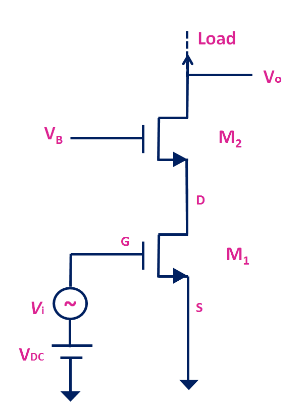
A Cascode Amplifier is a two-stage multistage amplifier consisting of a Common Emitter (CE) stage feeding into a Common Base (CB) stage.
(Note: In Field Effect Transistor (FET) terminology, this corresponds to a Common Source driving a Common Gate.)
A Bipolar Junction Transistor (BJT) is a solid-state device where the current flow between two terminals (the Collector and the Emitter) is controlled by the amount of current flowing through a third terminal (the Base).
BJTs are fundamental to analog circuits, especially in very-high-frequency applications such as Wi-Fi systems and radio transmitters. They can also be combined with MOSFETs in BiCMOS technology to create integrated circuits that leverage the high speed of BJTs and the low power consumption of FETs.
Historical Context: The BJT was invented in December 1947 at Bell Telephone Laboratories by John Bardeen, Walter Brattain, and William Shockley. This invention replaced fragile, power-hungry vacuum tubes with tiny, rugged silicon devices, revolutionizing the electronics industry.
A BJT consists of a three-layer "sandwich" of doped semiconductor materials. The three layers are the Emitter, Base, and Collector.
The physical arrangement of these layers defines the two primary types of BJTs:
The practical difference lies in the polarity of the voltages and the direction of current flow.
Comparison Table:
| Feature | NPN Transistor | PNP Transistor |
|---|---|---|
| Structure | Two N-type layers sandwiching one P-type layer. | Two P-type layers sandwiching one N-type layer. |
| Majority Carriers | Electrons | Holes |
| Current Flow | Collector to Emitter | Emitter to Collector |
| Collector Voltage | Positive (relative to Emitter) | Negative (relative to Emitter) |
| Bias Configuration | Base-Emitter Forward, Base-Collector Reverse. | Base-Emitter Forward, Base-Collector Reverse. |
| Symbol Arrow | Points Out (Not Pointing In) | Points In (Pointing In) |
| Switching Speed | Faster (Electrons move faster than holes) |
| Slower |
| Symbol | 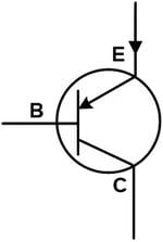 | 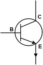 |