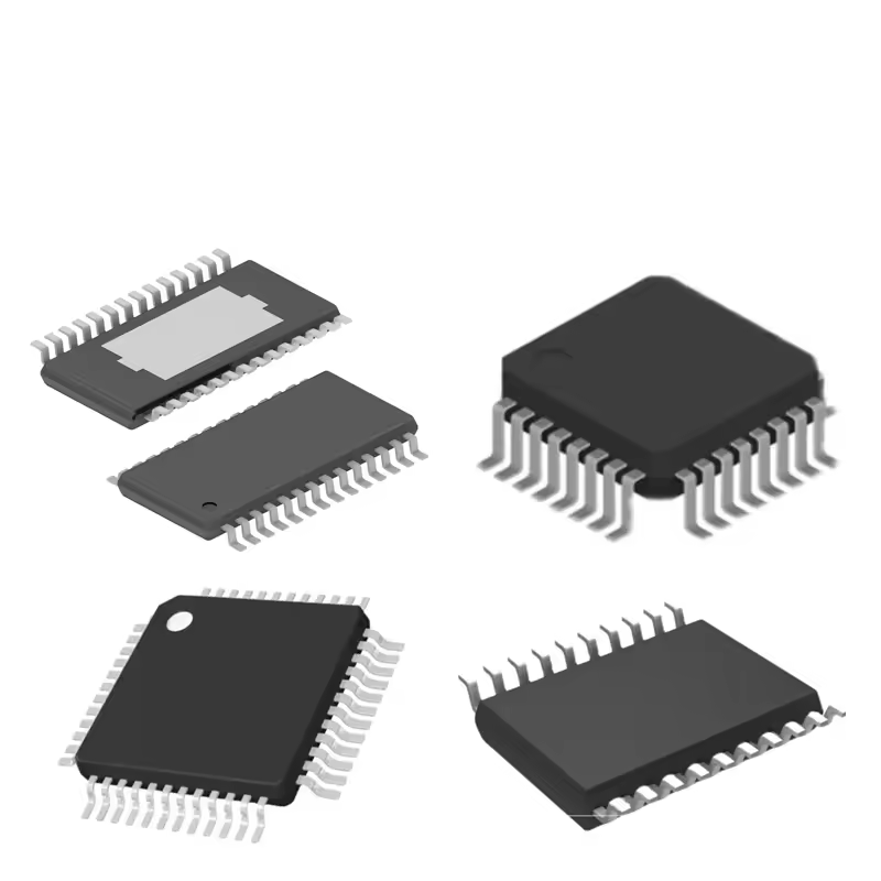
| Type | Description | ||
|---|---|---|---|
| Output | Single | Iq Typ (mA) | 0.145 |
| Noise (µVrms) | 50 | IO Typ (A) | 0.3 |
| Package Type | TSOP-5 / SOT-23-5 | MSL Type | 1 |
| MSL Temp (°C) | 260 | Container Type | REEL |
| VI Max (V) | 6.5 | VDO Typ (V) | 0.187 |
| PSRR (dB) | 55 | Enable | Yes |
| Container Qty. | 3000 | Polarity | Positive |
| VO (V) | 2.5 | VI Min (V) | 1.8 |
| PowerGood | No | Case Outline | 483 |
YG GROUP (YUGUANG INTERNATIONAL(HK)CO.,LTD) supports reliable sourcing through quality controls and compliance documentation. Please confirm product requirements, applicable certifications and supporting documents before ordering.
NCP603SN250T1G is an authentic electronic component manufactured by onsemi, categorized under Power Management ICs. It is supplied in the standard manufacturer-specified package footprint, providing industry-standard mechanical dimensions and terminal configurations for board-level assembly. Full pinout configurations, physical footprint drawings, and rated operating tolerances are documented in the official NCP603SN250T1G datasheet above.
Electronic component spot-market pricing for NCP603SN250T1G fluctuates based on real-time global availability, production date codes, minimum order quantities (MOQ), and packaging formats (e.g., Reel, Tube, Tray). Using an RFQ ensures you receive accurate, real-time volume pricing tied to verified, traceable inventory rather than stale catalog estimates.
Lead times for NCP603SN250T1G depend on whether stock is dispatched from our central hub or regional franchise partners. Ready-to-ship inventory typically leaves the warehouse within 1–3 business days following quality inspection, while factory-direct or back-ordered allocations are confirmed with an estimated ship date upon RFQ reply.
Loading articles…

Loading articles…

Verify TLF35584QVVS2 voltage variant, C13/C14 order codes, VQFN-48 package and firmware approval records without assuming safety-system compatibility.
Read more →
Budget AD8251ARMZ gain-latch timing, analog settling and ADC acquisition separately. Check the falling WR edge, REF pin 9 and the limits of a 785 ns figure.
Read more →
Plan AD9361BBCZ complex sample rates, occupied bandwidth and two-channel I/Q payload. Separate calculated budgets from validated filter and interface modes.
Read more →
Size FDD4141 gate pull-up and clamp networks using the ±20 V VGS limit, verified DPAK pins, current-rating conditions, and rail-transient checks.
Read more →Loading related products…
| Picture | Part Number | Manufacturer | PDF / RoHS | Stock | Action |
|---|---|---|---|---|---|
| onsemi | 2,740 | |||
| onsemi | 7,230 | |||
| onsemi | 8,230 | |||
| onsemi | 7,180 | |||
| onsemi | 3,300 | |||
| onsemi | 4,950 | |||
| onsemi | -- | 3,040 | ||
| onsemi | 4,010 | |||
| onsemi | 8,620 | |||
| onsemi | 4,450 |
