
Susanna Feng




| Picture | Part Number | Manufacturer | Stock | Action |
|---|---|---|---|---|
 | TLF35584QVVS2 | Infineon | 4,120 | |
 | TLF35584QVVS1XUMA2 | Infineon | 2,590 |
No. VS2 is the 3.3 V MCU/standby voltage variant. Infineon’s 2022 presentation separately maps XUMA1 to C13 and XUMA2 to C14 for the QV variants.
The presentation lists TLF35584QVVS2XUMA1 for C13 and TLF35584QVVS2XUMA2 for C14. Keep the document date and the approved BOM with this mapping; it does not authenticate a particular reel.
No. QT1 and QT2 track the 5 V reference regulator QVR. QUC is the VS2 3.3 V MCU output, and those relationships must match the approved board architecture.
No. Compatibility requires the relevant technical documents, errata, board revision, firmware build and validation records. The public overview and design-step table do not supply a universal initialization sequence or system safety approval.
By Susanna Feng | YG GROUP
TLF35584QVVS2 procurement must distinguish the VS2 voltage variant from the C13/C14 design step and the complete order code. Infineon’s 2022 presentation maps XUMA1 to C13 and XUMA2 to C14; that identification does not by itself qualify board firmware.
Infineon's public Product Overview describes the regulator architecture and package. Its October 2022 product presentation adds a useful design-step table: XUMA1 is associated with C13 and XUMA2 with C14. These documents support identification, but they do not replace the full technical datasheet, relevant errata, safety manual or the validation records for a particular ECU. Infineon presentation, page 17.
VS2 identifies the variant with a 3.3 V MCU supply and 3.3 V standby output. VS1 provides 5 V for those outputs. The letters are not interchangeable with the C13/C14 design-step identifiers. A request for “TLF35584, latest version” leaves both the voltage and order-code requirements ambiguous.
Table 1. Verified full order codes and public stepping information | Source: manufacturer documents in References; assumptions and operating conditions are stated in the table or adjacent text. Compiled / calculated by: YG GROUP.
| Complete order code | Design step in the 2022 presentation | MCU / standby outputs |
|---|---|---|
| TLF35584QVVS2XUMA1 | C13 | 3.3 V / 3.3 V |
| TLF35584QVVS2XUMA2 | C14 | 3.3 V / 3.3 V |
| TLF35584QVVS1XUMA2 | C14 | 5 V / 5 V |
The presentation lists order number SP001096172 for VS2 XUMA1 and SP001657936 for VS2 XUMA2. Those identifiers help reconcile a historical BOM, purchase record and manufacturer documentation. They do not prove the provenance of a specific reel, and the presentation's design-in preference reflects its 2022 issue date rather than a perpetual supply guarantee.
For incoming material, compare the exact OPN on the supplier documentation and packing label with the approved BOM. Retain the manufacturer order number where available, the lot and date information and the chain of purchase documents. A shortened invoice line should be clarified before material enters a controlled build.
The VS2 MCU regulator QUC is specified at 3.3 V with 600 mA capability in the overview. QST is the 3.3 V standby output. The communication supply QCO and reference supply QVR are 5 V outputs. QT1 and QT2 track the reference supply QVR; they should not be described as tracking the 3.3 V MCU rail.

Figure 1. VS2 output relationships from the public overview. Current figures describe output capabilities and do not establish every simultaneous-load operating condition. Source: manufacturer documents in References; calculation / diagram: YG GROUP.
The PMIC can support an external core post-regulator through control and monitoring functions. That does not make QUC an automatically suitable low-voltage core supply for any MCU. Compare the actual MCU rail requirements, sequencing and external regulation with the approved schematic.
The public architecture includes voltage supervision, watchdog functions, SPI communication, reset and safe-state signaling. The documented signal names include ERR, ROT, SS1 and SS2. Invented signal names or a generic block copied from another PMIC can conceal a wiring discrepancy, so use the exact document and approved schematic when checking the interface.
Identifying C13 or C14 does not establish that an existing binary is suitable for both. The design-step table does not enumerate all register behavior or errata. A compatible firmware claim should be tied to the full technical document revisions, the board revision, the released initialization code and the validated safety configuration.
A practical receiving decision begins by asking whether the delivered OPN is listed on the approved BOM or an authorized change notice. If it is a different step or variant, route it through the engineering change process. Compare initialization settings, watchdog service, reset behavior and fault handling against the applicable manufacturer documents before accepting it for production.
The release evidence should include startup across the specified rail conditions, watchdog service and response to defined faults. Specify which firmware build and board were tested, along with the environmental conditions and pass criteria. These are validation tasks for the product team; this article does not report that those tests were performed or supply a substitute register sequence.
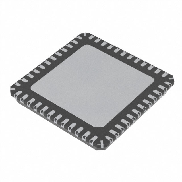
The QV version in the overview uses PG-VQFN-48. Its nominal body is 7 mm square with a nominal 5.2 mm exposed pad; both are shown with ±0.1 mm tolerances in the package drawing. The nominal exposed-pad dimension should not be replaced by its 5.1 mm minimum when describing the package.

Figure 2. Package-identification geometry, not an electrical pin map or manufacturing footprint. Use the released package and land-pattern documents for fabrication. Source: manufacturer documents in References; calculation / diagram: YG GROUP.
The QK family uses a different LQFP-64 package in the same official presentation. It must not be classified as merely another finish of the same 48-terminal footprint. Package appearance can support a discrepancy check, but matching appearance alone does not establish authenticity or electrical suitability.
Preserve the original moisture-barrier and handling information supplied with the material. Apply the qualified receiving and assembly procedure to the actual label and package status. An assumed universal bake temperature or duration is unsuitable because it ignores exposure history, carrier material and the applicable handling instruction.
Table 2. Related PMIC output-voltage comparison | Source: manufacturer documents in References; assumptions and operating conditions are stated in the table or adjacent text. Compiled / calculated by: YG GROUP.
| Candidate | Confirmed difference | Purchasing implication |
|---|---|---|
| TLF35584QVVS2XUMA2 | C14; 3.3 V MCU and standby variant | Match the approved complete OPN and firmware release |
| TLF35584QVVS1XUMA2 | C14; 5 V MCU and standby variant | Reassess electrical rails; do not substitute on family name |
Safety features intended to support an ASIL-D system do not certify the finished controller by themselves. The product's safety concept, integration assumptions and evidence remain part of the system approval. Similarly, a verified order code does not establish current availability or guarantee future lifecycle status.
For YG GROUP procurement records, keep the approved OPN, manufacturer sources, board and firmware identifiers, supplier traceability and disposition of any discrepancy together. That record gives purchasing and engineering a common basis for accepting the delivered material without turning a short part-name match into an unsupported compatibility promise.