
Kelsey Lee




| Picture | Part Number | Manufacturer | Stock | Action |
|---|---|---|---|---|
 | XC7Z010-1CLG400I | Xilinx | 6,490 | |
| XC7Z020-1CLG400I | Xilinx | 4,840 | |
| XC7Z007S-1CLG400I | Xilinx | 8,880 | |
| XC7Z014S-1CLG400I | Xilinx | 8,070 | |
 | XC7Z015-1CLG485I | Xilinx | 8,340 |
No. SEMI's July 13, 2026 announcement describes global Q1 2026 revenue for electronic design automation, semiconductor IP, and services. It does not report unit shipments, inventory, or customer purchases of this exact chip. The data can frame a discussion about design tools and reusable IP, but it cannot establish component demand, price, or lead time. Those decisions require separate current evidence for the complete ordering model. The SEMI announcement is industry context, not a device availability report.
XC7Z010-1CLG400I identifies the XC7Z010 device, −1 speed grade, CLG400 package, and industrial temperature option. DS190's ordering and package information, together with DS187's applicable speed and temperature tables, supports that interpretation. The industrial range is −40°C to +100°C junction temperature, not an ambient guarantee for a whole board. Select the matching implementation target and evaluate the actual power and cooling conditions. Results obtained for a faster speed grade, a different package, or the separate −1LI operating option cannot simply be carried across.
Possibly, if the necessary archived design data and generated outputs are intact and the documented workflow applies. AMD describes retaining certain older or selectively upgraded IP through existing checkpoints, with restrictions on editing and regeneration. A locked status therefore needs investigation, rather than an automatic conclusion that the project is unusable. Preserve the known build, review IP status and change logs, and decide whether the task requires an unchanged build or a modified subsystem. Follow the UG896 selective-upgrade guidance for the actual tool release and available artifacts.
By Kelsey Lee
XC7Z010-1CLG400I combines an Arm processing system with programmable logic, making design reuse a practical consideration for embedded teams. Reusing an existing subsystem can preserve useful engineering work, but the decision depends on the exact device, software environment, IP configuration, and board interfaces. Growth in electronic design software and semiconductor IP revenue provides industry context. It does not prove demand, availability, or a price trend for this particular AMD-Xilinx ordering model.
SEMI's ESD Alliance reported global electronic system design revenue of US$5,747.8 million for Q1 2026, up 12.7% from Q1 2025. Semiconductor IP revenue was US$2,332.5 million, up 14.1%. The July 13, 2026 announcement covers EDA, semiconductor IP, and services, rather than FPGA shipments. Q1 2026 was the current edition identified on SEMI's market-data page when checked on September 22, 2026. These figures establish the scale and growth of the design ecosystem; they do not identify which chips participating customers purchased. SEMI announcement; Electronic Design Market Data.
*Figure 1. Conceptual XC7Z010-1CLG400I subsystem review. Software, AXI interfaces, clocks, resets, memory, and board connections are separate contracts; the diagram is not a verified customer design or a package pinout.* *Figure 2. Proposed decision gates for XC7Z010-1CLG400I reuse. A missing artifact or failed check returns the relevant work for correction; the flow reports no measured schedule savings or completed qualification.*No. Validate Design checks the block design and can propagate parameters and expose integration errors. It does not establish completed timing closure, correct software behavior, acceptable power, or reliable operation on an assembled board. Continue with implementation reports, interface tests, software regression, and measurements under realistic workloads. In particular, confirm addresses, clock and reset assumptions, data representation, and buffer behavior across the processing-system and programmable-logic boundary. Keep the tool's validation result as one piece of evidence in the qualification record.
Not when it depends on dedicated GTP resources that XC7Z010 does not contain. DS187's GTP sections apply to XC7Z012S and XC7Z015 among the low-density devices it covers. A project using those resources needs a different hardware selection or a redesigned interface. A common family name or similar block diagram cannot supply missing physical resources. Check the required transceiver, package connections, clocking, and protocol implementation before assuming that a reusable core can be placed on this target.
XC7Z020-1CLG400I, XC7Z007S-1CLG400I, XC7Z014S-1CLG400I, and XC7Z015-1CLG485I address different design needs. The first offers a larger dual-core family option; the two S devices use a single-core processor with different logic capacities; XC7Z015 adds GTP resources in a different package. AMD's device/package tables and ordering fields support these combinations. None is established here as a direct substitution. Revisit resources, software concurrency, pin and bank assignments, power, timing, and board interfaces for whichever candidate matches the product's requirements.
Table 1. Keep the market observation separate from the device decision.
| Observation | Period and scope | Appropriate use | Unsupported inference |
|---|---|---|---|
| ESD revenue grew 12.7% year over year | Global Q1 2026 reporting; EDA, semiconductor IP, and services | Context for investment in design capabilities | XC7Z010-1CLG400I unit demand grew by the same amount |
| Semiconductor IP revenue grew 14.1% year over year | Global Q1 2026 category within the same report | Context for reuse-oriented engineering discussions | A particular core or device will reduce this project's cost |
| A device-specific reuse review is still required | The actual project, tool release, and board | Decide which existing assets remain usable | Market growth establishes stock, lead time, or compatibility |
The engineering question is narrower and more useful: which parts of an existing design can be carried into a new XC7Z010-1CLG400I product with evidence? An algorithm, an AXI peripheral, a board preset, and a complete boot image are different reuse assets. Each carries different assumptions. Treating them as one ready-made platform can hide the work required at their boundaries.
A team may save substantial effort by retaining a well-tested signal-processing block while rebuilding its board interface. Another team may find that an old project opens successfully but depends on unavailable generated files or a configuration that no longer matches the hardware. Neither outcome follows from market revenue. They follow from the quality of the archived design and the differences between the old and new requirements.
Use the industry news as a reason to ask better questions about reusable assets. Ask who maintains the core, which tests travel with it, how its interface is documented, and what evidence supports its resource and timing claims. That turns a broad trend into a concrete engineering review without pretending that aggregate spending forecasts a specific component's supply position.
The target in this article is XC7Z010-1CLG400I: the XC7Z010 device, speed grade −1, CLG400 package, and industrial temperature designation. The Zynq-7000 overview, DS190, provides device/package selection and ordering information; DS187 v1.21 provides the applicable electrical and switching conditions. Together they support the ordering-code interpretation. The industrial junction-temperature range is −40°C to +100°C, rather than an ambient-temperature promise for a complete board.
That last distinction is easy to overlook in a reuse discussion. A previous enclosure, airflow arrangement, or processing load can change junction temperature even if the room-temperature environment stays the same. The component's temperature grade does not establish that a smaller enclosure will dissipate heat adequately. Reuse the thermal assumptions only when the new power and cooling conditions support them.
The XC7Z010 processing system uses two Cortex-A9 cores. Its programmable logic offers roughly 28,000 logic cells and 80 DSP slices. These family-selection figures are useful for an initial fit assessment, but implementation reports describe what a particular design actually consumes. A saved project targeting a larger family member should not be treated as an XC7Z010 design merely because its processor architecture looks familiar. AMD Zynq 7000 product tables.
Table 2. XC7Z010-1CLG400I boundaries that a reused project must preserve.
| Item | Applicable fact | Reuse consequence | Primary evidence |
|---|---|---|---|
| Device and package | XC7Z010 in CLG400 | Resource selection, package pins, and board constraints must agree | DS190 device/package and ordering tables |
| Speed grade | −1 | Re-run timing with the intended grade; faster-grade results cannot be inherited | DS187, pp. 13–15 |
| Temperature | Industrial junction range −40°C to +100°C | Check junction temperature under the new workload and cooling arrangement | DS187, Table 2 |
| Standard PL core supply | Nominal 1.0 V; recommended 0.95 V to 1.05 V | Do not apply the separate −1LI low-voltage operating mode | DS187, Table 2 and speed-grade notes |
| CPU clock limit | 667 MHz maximum at the 6:2:1 clock ratio | A family headline does not replace the selected speed-grade limit | DS187, Table 17 |
| Dedicated GTP transceivers | Not present in XC7Z010 | Transceiver-dependent subsystems require a different hardware choice or architecture | DS187, pp. 61–67; DS190 selection tables |
The −1 designation is especially relevant when a demonstration design advertises a clock rate. DS187 gives a maximum CPU clock of 667 MHz for the relevant −1 column at the 6:2:1 ratio, and a different limit at the 4:2:1 ratio. BootROM execution has its own limit. A single frequency copied from a family webpage cannot describe all of those operating states.
The same discipline applies to power. Standard −1 operation and the separate −1LI low-voltage option are not interchangeable. A reused regulator configuration must match the actual ordering model and all connected rails. DS187 also distinguishes processing-system and programmable-logic power behavior. A successful design on one board is evidence about that board and configuration, not permission to alter rail voltages without another review.
Start the project record with the complete commercial ordering code and the corresponding tool target. Keep package, speed, and temperature assumptions visible even when a tool represents them in separate settings or a shorter identifier. That gives hardware, firmware, procurement, and verification teams a common reference and makes later substitutions easier to assess.
A reusable IP block needs more than a name and a block-diagram screenshot. Preserve its source or configuration, exact version, generated outputs where required, constraints, simulation dependencies, and the tool release that produced the known working build. Record where external repositories or licensed cores enter the flow. The purpose is to make another engineer capable of reproducing the result without guessing which files were on the original workstation.
AMD's UG896 guidance on upgrading IP recommends archiving projects before an upgrade and reviewing IP status and change information. Upgrading can remove previously generated output products, including checkpoints and associated runs. The practical consequence is straightforward: preserve the known build before experimenting with a new release, and compare the changed design against it afterward.
A version change deserves review even when the graphical symbol looks the same. Parameters, generated wrappers, timing constraints, and integration behavior can change without altering the broad function described by the icon. Identify which differences affect the surrounding design and which are administrative. Then choose tests that exercise the affected behavior instead of relying entirely on whether synthesis completes.
Table 3. A reusable subsystem handoff should include these artifacts.
| Artifact | Question it answers | Failure exposed when missing |
|---|---|---|
| Exact part and tool-release record | What implementation environment produced the baseline? | A build silently targets a different package or speed grade |
| IP version and parameter configuration | What functionality was actually generated? | A recreated core has different widths, options, or address behavior |
| Source and required generated outputs | Can the design be reconstructed on another workstation? | The archive depends on an untracked local file |
| Constraints and interface contract | What clock, reset, I/O, and timing assumptions apply? | A functionally correct block is integrated outside its assumptions |
| Test inputs and expected results | Which behaviors were verified? | A new build passes compilation but changes application behavior |
| License and ownership record | What access and permitted use must the project maintain? | The team cannot reproduce or use a required core under its actual entitlement |
Use this handoff to identify missing dependencies before changing the project. Its contents are proposed review items; acceptance still requires results from the actual build.
License review should be specific to each IP core and the organization's entitlement. The existence of a component in an IP catalog does not establish all usage rights, and the ability to simulate a core does not by itself establish the same access for every later build step. Record the applicable license information and its owner, then resolve uncertainties through the relevant vendor process. Avoid building a schedule around an assumed entitlement that nobody has checked.
A locked IP status also needs interpretation rather than a reflexive upgrade. AMD describes a selective-upgrade flow that can retain locked, unmodifiable checkpoints when the necessary previously generated outputs are available. That is a conditional workflow, not a universal guarantee that every old block can be edited or regenerated in a newer release. Decide whether the project needs preservation, modification, or a full upgrade before changing it.
AMD's block-design release guidance similarly distinguishes retaining intact older design data from upgrading and regenerating a design. For a maintained product, document which route was selected and why. An unchanged manufacturing build and a redesigned subsystem may reasonably follow different routes, provided each retains reproducible evidence.
The most useful unit of reuse is often a subsystem with a clear contract. For a processing-system-controlled accelerator, that contract includes register addresses, access widths, interrupts, buffer ownership, clocking, reset behavior, and error reporting. The processing system and programmable logic may compile separately while disagreeing about one of those details. A successful hardware build alone does not establish that software is using the new subsystem correctly.
Consider a conceptual acquisition product in which software configures an input-processing block and receives processed samples. The block may preserve its numerical algorithm when moved between projects, yet require a new bus adapter, different buffering, or a changed reset sequence. Keeping the algorithm test separate from the integration test makes those differences easier to diagnose. It also gives reuse a precise meaning: the numerical function is retained while the interface is revalidated.
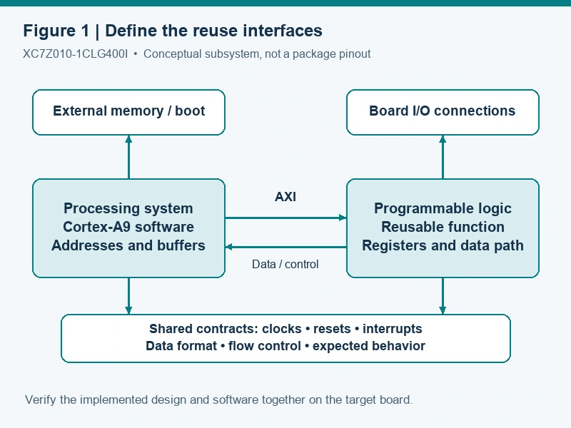
Begin with addresses. Confirm that each software-visible block has the expected base address and range, and that generated software descriptions match the exported hardware design. A register read from an old address can look like an unresponsive peripheral even when the new core is working properly elsewhere. Retain a small access test that reads known identification or status behavior before relying on the full application.
Next review data representation. State byte order, signedness, sample width, alignment, and any scaling that crosses the boundary. A reused arithmetic block may pass its own simulation while software interprets its output with an old conversion factor. Include representative negative values, boundary values, and overflow behavior in the interface tests. These are inexpensive checks compared with debugging plausible but wrong measurements after system integration.
Clocks and resets need similarly explicit ownership. Identify which domain produces each clock, which blocks depend on it, and how reset behaves when that clock is absent or changes. Check crossings between domains as part of the implemented design. Copying a reset wire from a previous diagram does not establish safe startup for a new clock structure, especially when software now configures clocks in a different order.
AMD's IP-subsystem validation guidance explains that Validate Design applies block-design checks and triggers parameter propagation. It can catch errors such as an incorrectly specified clock frequency. Run it after meaningful integration changes, review its messages, and inspect propagated values. It is one layer of verification; it does not replace implementation timing, software tests, or measurements on the assembled board.
Memory traffic deserves its own workload description. State how much data arrives, how bursty it is, how long software can be delayed, and what the system should do when a buffer fills. Then test those cases. A core's peak transfer capability says little about an application that shares memory and processor time with other tasks. Reuse should preserve the assumptions behind throughput claims, or explicitly replace those assumptions with new evidence.
Interrupt behavior can also change the apparent reliability of a reused block. Confirm how an event is acknowledged, whether multiple events can accumulate, and what happens while software is servicing another task. A test that triggers one event after a long idle interval may miss a problem that appears only during sustained operation. Define the required event rate and acceptable loss behavior before judging the integration complete.
DS187 contains many timing values, but each belongs to a specific interface, speed grade, or test condition. They are not one interchangeable performance rating. The distinction between the processing-system DDR controller and a memory interface implemented in programmable logic is particularly relevant: their limits appear in different tables. A reused memory subsystem must be checked against the table and implementation that actually applies.
For the relevant −1 column, DS187 Table 18 lists PS DDR3 and DDR3L interface performance up to 1066 Mb/s. Table 51 gives separate PL memory-interface limits with controller-ratio and memory-standard conditions. The numbers are data rates, not promises of sustained application bandwidth. Board routing, memory choice, initialization, arbitration, and the implemented workload still determine the useful system result.
Table 4. Verification evidence to request before accepting the reused design.
| Area | Evidence to review | Boundary that prevents an invalid shortcut |
|---|---|---|
| Target and timing | Implementation reports for the selected device, package, and −1 grade | Results for a faster grade or larger device do not qualify this target |
| Power and temperature | Rail measurements, workload-based power estimate, and thermal evaluation | Blank-device quiescent current is not operating-system power |
| DDR interface | Correct PS or PL configuration, memory settings, and board-level tests | PS and PL memory tables describe different interfaces |
| I/O and package | Pin assignments, bank supplies, standards, loading, and external timing | A shared package name does not prove identical usable connections |
| Startup and reset | Recorded rail ramps, reset timing, and boot behavior | A warm reset does not establish cold-start performance |
| End-to-end function | Hardware/software regression under realistic traffic | Block-design validation alone does not prove the application works |
Source boundaries: DS187 Tables 2, 17–23, 25–36, 51, and 84, together with AMD's documented IP validation flow. The requested tests are proposed acceptance evidence, not results from this article.
Power estimates should use the intended clock rates, resource activity, I/O loading, and processing workload. DS187's typical quiescent values describe a defined blank configuration and temperature; multiplying one of those values by a rail voltage does not establish the consumption of an active embedded product. Record the assumptions behind an estimate and refine them when implementation activity and board measurements become available.
At startup, review the actual power sequence and reset waveform together. DS187 gives a minimum PS_POR_B assertion interval after the relevant PS supplies reach their minimum levels and also describes a secure-lockdown timing relationship to PL ramping. A copied reset delay is therefore insufficient evidence by itself. Check the applicable conditions rather than taking a single timing number out of the surrounding sequence.
External interfaces have equally specific conditions. The QSPI timing table distinguishes feedback-clock operation and capacitive loading. RGMII timing is stated for particular I/O voltage and drive conditions. If a reused board design changes the memory placement, external device, voltage standard, or trace loading, revisit the interface budget even when the protocol name stays the same. Protocol compatibility does not erase electrical timing requirements.
Package timing is another reminder that physical implementation matters. DS187's package-skew table lists device/package combinations separately. It supports timing-budget work; it is not a pin-compatibility certificate. Compare the selected pinout and bank functions directly when considering another device, and keep any board-level migration claim narrower than the evidence actually reviewed.
For a meaningful performance test, define both success and failure observations. Average throughput may meet the target while worst-case latency does not. A design may pass a short test before buffers fill, or pass at room temperature while approaching its thermal limit under a sustained workload. Match test duration, traffic, and environment to the product's requirements, and preserve the conditions with the results.
The four models below are related family members chosen to expose useful reuse tradeoffs. Their identities are supported by the manufacturer's device/package choices and ordering fields, cross-checked against DS187's speed and temperature coverage. The combinations follow AMD's documented device, package, speed-grade, and temperature options. Confirm current orderability when sourcing; the comparison establishes neither stock nor direct substitution.
Table 5. Four related ordering models and their migration questions.
| Related exact model | Shared architectural basis | Meaningful difference from XC7Z010-1CLG400I | Reuse boundary |
|---|---|---|---|
| XC7Z020-1CLG400I | Dual-core Cortex-A9 processing system with programmable logic | Larger programmable-logic resource set in a CLG400 option | Rebuild and review pin, bank, power, timing, and resource assumptions |
| XC7Z007S-1CLG400I | Zynq-7000 processing-system and programmable-logic architecture | Single-core processor and smaller programmable-logic resource set | Review software concurrency and implementation fit |
| XC7Z014S-1CLG400I | Zynq-7000 processing-system and programmable-logic architecture | Single-core processor with more programmable logic than XC7Z010 | More logic does not preserve dual-core software behavior |
| XC7Z015-1CLG485I | Dual-core Cortex-A9 processing system with programmable logic | Different package and dedicated GTP resources | Board redesign and transceiver-specific integration review are required |
Sources: AMD/Xilinx DS190 device, package, and ordering tables; DS187 speed-grade coverage and GTP applicability; AMD Zynq 7000 product selection tables. All four are related candidates. No direct substitution or pin compatibility has been established here.
A larger programmable-logic device may preserve the high-level design while changing placement, routing, timing, and power. A smaller option may require removing features or restructuring the implementation. The decision should therefore use synthesis and implementation evidence from the proposed target, not a proportional estimate based only on logic-cell counts. Different resource types can become the limiting factor at different stages.
The single-core models deserve a separate software review. An application originally divided across two processor cores may need a new scheduling arrangement even if the programmable logic fits well. Identify which behavior depends on parallel execution, interrupt affinity, or processor availability. Reusing source code is different from preserving its timing behavior under the same workload.
The XC7Z015 candidate changes a different boundary. Its GTP capability can matter for a serial-link requirement that the XC7Z010 cannot satisfy directly. That benefit arrives with a different package and interface work, so it should be considered an architectural migration. Conversely, an existing design containing a transceiver-dependent core cannot be assumed to work on XC7Z010 merely because both parts are in the same family.
Estimate reuse effort by work package: archive recovery, tool migration, IP changes, board adaptation, software integration, and verification. Assign an owner and a completion condition to each. This makes the estimate reviewable without inventing a universal percentage saving. A subsystem with complete tests and clear interfaces may be easier to reuse than a larger collection of undocumented code, even when both appear equally functional in a demonstration.
Separate mandatory work from optional modernization. A changed package or invalid timing assumption must be resolved for the new product. A cosmetic refactoring of an otherwise reproducible subsystem may be scheduled differently. Keeping those choices visible helps avoid a project that expands silently while still being described as simple reuse.
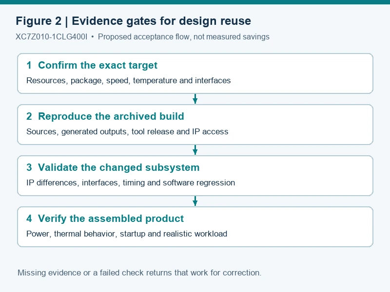
At the first gate, confirm that the target has the resources and physical interfaces the product requires. At the second, reproduce the archived build in a controlled environment. At the third, resolve IP and integration changes and run the relevant regressions. At the final gate, verify the assembled hardware under realistic power, thermal, timing, and workload conditions. Evidence from one gate should not be used to waive a different gate's question.
For an arithmetic subsystem, preserve reference vectors that exercise the actual numerical format. Include values near saturation, sign changes, and any rounding boundary that matters to the application. If a migration changes pipeline depth, compare both the result and its timing relationship to valid signals. A correct value on the wrong cycle can still corrupt a larger processing chain. Write down whether the acceptance criterion requires identical bits or an explicitly allowed numerical tolerance, and explain the reason for that choice.
For the board interface, count the required signals before committing to a package. Include clocks, control lines, interrupts, debug access, and future connections that are actual product requirements. Then group them by voltage and bank constraints rather than treating the available pins as one interchangeable pool. A design can have enough pins in total yet lack a suitable arrangement for the required interfaces. Resolve that placement early, before an attractive resource comparison turns into an expensive board revision.
For the build itself, keep machine-generated reports with the source revision that produced them. Record which warnings were reviewed and why any remaining warning is acceptable. A later successful run can otherwise overwrite the evidence for an earlier release, leaving the team unsure whether a reported improvement came from source changes, tool changes, or different settings. This small discipline makes future comparisons much more useful.
Keep a short decision record at release. It should identify the exact ordering model, hardware revision, tool release, IP versions, software baseline, open limitations, and the tests that support acceptance. That record becomes the starting point for the next reuse effort. Without it, the next team has to rediscover which parts of the design were assumptions and which were actually demonstrated.
Procurement belongs alongside that record, with its own current evidence. Confirm the complete requested model, packaging, traceability requirements, and delivery conditions when sourcing. An older datasheet or a market-growth announcement does not establish available inventory. Likewise, a sourcing proposal for a different family member should return to the engineering comparison before it is accepted as an equivalent build option.
The value of reuse on XC7Z010-1CLG400I comes from retaining verified behavior and making the remaining changes explicit. Industry growth gives context to the tools and IP ecosystem. The decision for a real product rests on a reproducible build, compatible interfaces, the correct electrical limits, and board-level evidence for the intended workload.