
Zoey Zhou




| Picture | Part Number | Manufacturer | Stock | Action |
|---|---|---|---|---|
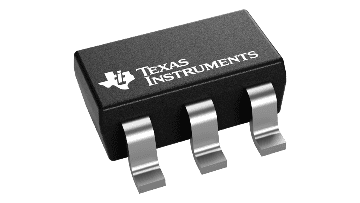 | REF35330QDBVR | Texas Instruments | 7,150 | |
| REF35250QDBVR | Texas Instruments | 9,860 | |
| REF35409QDBVR | Texas Instruments | 5,430 |
It is the typical quiescent current at 25 C. TI specifies 0.9 uA maximum at 25 C and 2.6 uA maximum across -40 to 125 C. The reference's output-load current adds a separate contribution. Use the relevant maximum for a worst-case temperature budget and account for the connected measurement chain.
Initial accuracy is +/-0.05% maximum at 25 C, corresponding to +/-1.65 mV at 3.3 V by arithmetic. The 12 ppm/C maximum temperature coefficient applies across -40 to 105 C. Functional operation extends to 125 C, but that wider limit does not extend the stated temperature-coefficient guarantee. ADC, sensor and calibration errors remain separate contributions.
The noise-reduction capacitor filters noise and changes settling; leakage at the NR node can affect accuracy. TI's illustrated start-up uses REF35250 with its stated capacitor arrangement. Evaluate the actual REF35330 circuit's enable-to-valid-reading interval using its chosen output load and NR/output capacitors rather than copying a different variant's curve.
Category: Manufacturer Insights
By Zoey Zhou
REF35330QDBVR is a 3.3-V reference with 650 nA typical quiescent current at 25 C. TI also specifies a maximum initial accuracy error of +/-0.05% at 25 C. Together, those figures give a low-power precision design a useful starting point. The purchasing specification still needs the operating and accuracy temperature intervals, reference loading and time available before the first measurement.
The reference sets a scale for the analog chain, so its contribution cannot be judged from supply current alone. The exact Texas Instruments order code uses the six-pin SOT-23 DBV package, with current and accuracy limits that can be carried into a purchasing specification. TI lists this code as Catalog; the Q in its name is not evidence of Q1 automotive qualification.
REF35250QDBVR and REF35409QDBVR retain the six-pin DBV family configuration and change nominal output to 2.5 V and 4.096 V. They are voltage-selection comparisons. Recheck ADC span, input headroom, analog limits, calibration and the full error budget; a common package does not preserve the original 3.3-V measurement scale.
Name REF35330QDBVR as the 3.3-V six-pin DBV Catalog option, quantity, need-by date and carrier requirement. Its Q character is separate from Q1 automotive qualification. For requested electrical checks, state temperature, loading, capacitor arrangement and settling time. Ask which source records and checks accompany the offered supply so the result corresponds to the intended measurement conditions.
The REF35 electrical table specifies 650 nA typical and 0.9 uA maximum quiescent current at 25 C. Over the -40 to 125 C operating range, the maximum becomes 2.6 uA. A battery-budget calculation based only on the typical room-temperature number leaves that difference unresolved. TI REF35 electrical characteristics, pp.5-6
Reference output current is also separate from quiescent current. An ADC, divider or other load drawing current from the reference still consumes energy, even when the reference's internal overhead is small. Engineering should identify the average and peak reference load in active measurement, standby and wake-up states.
For a hypothetical example, a 3.3-V source across two 47-kohm resistors draws about 35.1 uA continuously. That passive load is much larger than 650 nA. The arithmetic does not describe a particular REF35330 board; it illustrates why divider values and measurement duty cycle can dominate an otherwise attractive current figure.
Quote the reference against a system current allocation with stated conditions. If the requirement is a worst-case standby budget over temperature, the corresponding maximum is the relevant device figure. If the design switches the reference off between readings, the measurement sequence must include its recovery and settling behavior.
Table 1. Current and accuracy figures need their stated operating conditions
| REF35330 decision item | Conditioned datasheet value | Meaning for qualification |
|---|---|---|
| Output voltage | 3.3 V nominal | Match the ADC range, sensor scaling and available supply |
| Quiescent current | 650 nA typical at 25 C; 0.9 uA maximum at 25 C | Separate typical operating estimate from guaranteed room-temperature limit |
| Quiescent current over temperature | 2.6 uA maximum across -40 to 125 C | Use the appropriate bound in a full-temperature power budget |
| Initial accuracy | +/-0.05% maximum at 25 C | One contribution to the measurement error budget |
| Temperature coefficient | 12 ppm/C maximum across -40 to 105 C | Preserve the specified temperature interval |
| Low-frequency output noise | 3.8 ppm peak-to-peak typical at 25 C, 0.1-10 Hz, for output variants at least 2.5 V | Compare noise in the relevant measurement bandwidth |
Source: TI SNAS809C electrical-characteristics tables. Typical values are not maximum production limits.

Figure 1. Reference overhead and output load are separate budget items. TI specifies 650 nA typical and 0.9 uA maximum at 25 C, with 2.6 uA maximum over -40 to 125 C. The 35.1 uA divider load is a hypothetical 3.3-V calculation, not a measured REF35330 board.
At a nominal 3.3 V, an initial error of +/-0.05% corresponds arithmetically to +/-1.65 mV. It is an error contribution at the specified temperature, not the accuracy of a complete ADC measurement. Gain, offset, reference loading, temperature behavior, sensor variation and calibration residuals can add other contributions.
The 12-ppm/C maximum temperature coefficient is specified from -40 to 105 C. Extending that guarantee to 125 C because the device can operate there would change the source claim. Purchasing requirements should identify the actual accuracy temperature interval, which may differ from the wider functional operating range. TI electrical characteristics, pp.5-6
Noise should likewise carry its bandwidth and statistical basis. The electrical table gives 3.8 ppm peak-to-peak typical low-frequency noise at 25 C from 0.1 to 10 Hz for outputs of at least 2.5 V, including this 3.3-V version. The table's default setup uses VIN = VREF + 0.5 V, no output load, 10 uF output capacitance and 0.1 uF input capacitance. A single typical figure cannot represent every sampling rate or filter. Review the contribution that reaches the measurement through the actual analog and digital filtering.
An amplifier adds its own noise and gain conditions to the chain. Our OPA1612 noise-and-gain review follows that separate part of an analog budget, helping readers keep the reference contribution distinct from downstream amplification.
The six-pin DBV device provides a noise-reduction pin. Adding an NR capacitor filters the reference noise, but the capacitor and its leakage also deserve review. TI warns that leakage at this node can affect output accuracy, and added capacitance changes start-up behavior. NR description and device modes, pp.21-22
TI illustrates start-up using a REF35250 variant and specifies that output voltage, output capacitance and NR capacitance influence settling. That plot does not establish the start-up time of REF35330QDBVR with a different capacitor arrangement. Engineering should measure the delay from enabling the actual circuit to reaching the accuracy needed for its first valid reading.
The output-capacitor requirements also remain part of the design: TI specifies a 0.1-10 uF load-capacitance range and an ESR limit of 400 milliohms for the stated condition. A change in capacitor technology or effective capacitance should be reviewed with stability and load-transient behavior, rather than accepted simply because the footprint fits. Electrical conditions and basic connections, pp.6,22-23

Figure 2. Noise reduction, leakage and start-up must be evaluated together. Retain TI's stated 0.1-10 uF load-capacitance and 400-milliohm ESR conditions, then verify settling for the actual REF35330QDBVR circuit; no measured curve is shown.
REF35250QDBVR and REF35409QDBVR are meaningful related codes because they change the reference voltage to 2.5 V and 4.096 V. They retain the six-pin DBV package in TI's ordering tables. Package commonality simplifies an investigation but does not preserve the analog system's calibration. REF35 pin variants and ordering information, pp.3,34-35
Table 2. Related reference-voltage options change the measurement scale
| Complete ordering code | Nominal output | Comparison value | Boundary before approval |
|---|---|---|---|
| REF35330QDBVR | 3.3 V | Baseline reference for this review | Verify output load, supply headroom, noise and settling |
| REF35250QDBVR | 2.5 V | Lower-voltage measurement span | Recheck ADC input scaling, calibration and input supply |
| REF35409QDBVR | 4.096 V | Different measurement span and coding scale | Recheck input headroom, analog limits and complete error budget |
A reference swap can change the voltage represented by every ADC code. Firmware coefficients, sensor output range and overrange handling belong in the review even if the part's package and family remain familiar. These are engineering candidates, not calibration-preserving replacements.
A defensible REF35330QDBVR selection record names the required output voltage, qualification class, operating and accuracy temperature intervals, maximum current allocation, reference-load waveform and permitted settling delay. It should also identify the approved NR and output-capacitor arrangement.
REF35330QDBVR offers a low-current starting point for precision measurement; the complete power and error budgets determine its fit. Retain those conditions when comparing quotes or reference-voltage options. Engineering can then validate the same specification that purchasing uses, without turning a typical 650-nA figure into a battery-life or complete-measurement promise.
Request a REF35330QDBVR quotation from YG GROUP for the approved 3.3-V, six-pin DBV Catalog code. Include quantity, need-by date, packing and any lot/date-code requirements. Keep REF35250QDBVR or REF35409QDBVR separate unless a different measurement scale has been approved. Ask about available lot records and applicable checks; precision testing should use agreed temperature, load and settling conditions rather than a generic 'low-current' label.