
Jolin Zeng




| Picture | Part Number | Manufacturer | Stock | Action |
|---|---|---|---|---|
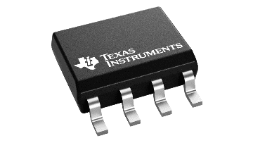 | OPA1612AIDR | Texas Instruments | 1,350 | |
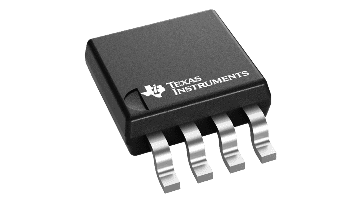 | OPA1602AIDGKR | Texas Instruments | 2,680 | |
 | OPA1611 | Texas Instruments | 4,900 |
No. It is a typical amplifier voltage-noise density at 1 kHz. The stage also includes source and resistor noise, current-noise contributions, frequency-dependent gain, and the measurement bandwidth.
No. Cable capacitance and the feedback arrangement can change phase margin. Use the intended load in analysis and transient testing, and evaluate any output isolation network as part of the complete signal path.
The supply span is within its recommended range, but the input common-mode and output-swing requirements must still be met. In particular, the specified input common-mode range at those rails is approximately 2–3 V; input biasing and amplitude must be designed accordingly.
No. Lower resistance can reduce thermal and current-noise contributions, but increases loading and may affect power and distortion. Select values that meet the complete stage requirement, then verify the physical implementation.
OPA1612AIDR is Texas Instruments’ dual bipolar-input audio operational amplifier in an eight-pin SOIC package. Its low voltage-noise density is most useful when source impedance, feedback resistance, gain, and measurement bandwidth are considered together. This guide develops that noise budget, then checks input headroom, output loading, protection, and layout so an amplifier selection becomes a defensible circuit decision rather than a comparison of isolated headline numbers.
An audio amplifier stage needs more than a target gain in decibels. Record the source's maximum and typical signal levels, its impedance across frequency, the load, the supply rails, and the required passband. Include the largest expected transient and the startup condition. These inputs determine whether the circuit has enough headroom and whether the op amp's noise is even the dominant contribution.
For OPA1612AIDR, the electrical table lists a typical input voltage-noise density of 1.1 nV/√Hz at 1 kHz, with a 1.5 nV/√Hz maximum at that frequency. It also lists typical input current-noise density of 1.7 pA/√Hz at 1 kHz. The voltage-noise number cannot be used alone because the current noise develops a voltage across the source impedance. Texas Instruments, SBOS450C, p.5.
The exact AIDR code selects the SOIC D package and large tape-and-reel packing. TI's orderable entry specifies 2,500 devices per standard carrier. The family datasheet also contains SON drawings, but those are not the footprint for OPA1612AIDR. Likewise, the single-channel OPA1611 has a different pin allocation even when its package is also SOIC-8. .
This is a useful place to separate engineering and purchasing records. The schematic may use the short family name OPA1612 for readability, but the released BOM should retain the full code, package, approved carrier, and assembly requirements. A visually similar suffix can change the assembly even when the analog function remains familiar.
For a unity-gain buffer driven through a purely resistive source, a simplified noise-density model combines three independent contributions:
e_total = sqrt(e_n² + (i_n × R_source)² + 4 × k × T × R_source)
Here, e_n is amplifier voltage-noise density, i_n is input current-noise density, R_source is source resistance, k is Boltzmann's constant, and T is absolute temperature. The result has units of V/√Hz. This is the buffer case discussed in TI's noise section; a gain-setting network adds further terms. SBOS450C, pp.15–16.
Table 1. Calculated buffer noise density for three source resistances. These are illustrative calculations, not measured OPA1612AIDR results or guaranteed limits. Assumptions: 300 K, purely resistive source, typical 1 kHz values e_n = 1.1 nV/√Hz and i_n = 1.7 pA/√Hz, uncorrelated sources, and no additional circuit noise. Formula basis: TI SBOS450C, pp.15–16. Calculated by YG Group.
| Source resistance | Resistor thermal noise | Current-noise contribution | Combined density |
|---|---|---|---|
| 100 Ω | 1.29 nV/√Hz | 0.17 nV/√Hz | 1.70 nV/√Hz |
| 1 kΩ | 4.07 nV/√Hz | 1.70 nV/√Hz | 4.55 nV/√Hz |
| 10 kΩ | 12.87 nV/√Hz | 17.00 nV/√Hz | 21.35 nV/√Hz |
The practical lesson is visible without ranking another amplifier. At 100 Ω, the op amp's voltage noise is a meaningful part of the total. At 10 kΩ, the current-noise term is much larger than 1.1 nV/√Hz. A design decision based only on that voltage-noise headline would miss the main contribution.
A real source may not look like a resistor. Microphone interfaces, coupling capacitors, filters, and volume controls can produce a frequency-dependent impedance. A potentiometer can also change its effective source impedance with position. Evaluate representative settings rather than calculating only at maximum volume or with the input shorted.
The shorted-input measurement remains useful, but it answers a narrower question: how the amplifier behaves with that low source impedance. It does not automatically predict the noise heard when the actual source and controls are connected.
Figure 1. OPA1612AIDR noise contributors as source resistance rises. Illustrative unity-buffer calculation using a purely resistive source at 300 K and typical 1 kHz amplifier densities of 1.1 nV/√Hz and 1.7 pA/√Hz. The stacked bars show fractions of noise variance, not linearly additive noise density. Independent terms combine by root-sum-square; frequency dependence, feedback noise and other circuit sources are excluded. These are not measured or guaranteed device results. Sources: supporting source 1.
For an ideal noninverting resistor stage, signal gain is 1 + R_feedback / R_ground. The same expression is its basic noise gain. For an inverting stage with a low-impedance source, signal gain is −R_feedback / R_input, while noise gain is 1 + R_feedback / R_input. Source resistance and reactive components modify the complete analysis.
This difference matters when comparing two circuits described simply as “gain of one.” A voltage follower and an inverting unity-gain stage do not present the same noise gain or resistor-noise contributions. The inverting circuit's input resistor also loads the source, whereas the noninverting arrangement has a different input-impedance behavior.
TI's Figure 33 gives separate equations for the two topologies and includes feedback-resistor noise and current-noise interaction. Use the equation for the actual circuit. Adding all resistor noise directly at the input without accounting for each transfer function can give a misleading result. SBOS450C, p.16.
For a noninverting gain of ten, 1 kΩ and 9 kΩ form one possible ratio; 10 kΩ and 90 kΩ form the same ideal ratio. They do not form the same noise circuit. Raising both resistances increases resistor thermal noise and changes the effect of current noise and parasitic capacitance. Lowering them reduces those noise terms but increases output loading through the feedback network.
The right resistor scale is therefore a tradeoff among noise, loading, bandwidth, distortion, and power. Choose it deliberately, then assess the actual tolerance and temperature behavior. A mathematically exact nominal ratio is not the same as a production gain-accuracy guarantee.
Avoid treating the 40 MHz unity-gain bandwidth figure as a promise that every gain setting will follow a simple, exact bandwidth division. The datasheet lists different gain-bandwidth behavior under different conditions and provides gain/phase curves. Use those curves and the relevant circuit model to examine the loop, especially when adding feedback capacitance or driving a capacitive load.
Figure 2. OPA1612AIDR unity signal gain does not imply unity noise gain. Ideal low-frequency resistor-stage comparison: a voltage follower has signal gain +1 and noise gain 1; an inverting stage with Rfeedback = Rinput and a low-impedance source has signal gain −1 and noise gain 2. Thus the amplifier input voltage-noise term alone is multiplied by one or two respectively. Total circuit noise also includes resistor noise, current noise and frequency-dependent transfer functions; this is not a measured OPA1612AIDR result or a bandwidth guarantee. Sources: supporting source 1.
Noise density and integrated noise describe different quantities. A density at 1 kHz is one point in a spectrum. An RMS noise voltage depends on the spectrum over the complete measurement bandwidth and on the transfer function applied to it.
For approximately white noise passed through an ideal rectangular bandwidth B, the simple estimate is V_noise,rms ≈ e_density × sqrt(B). A physical filter generally has an equivalent noise bandwidth different from its −3 dB frequency. Low-frequency noise, current-noise variation, and frequency-dependent gain also make the single-density approximation incomplete.
For illustration only, using 1.1 nV/√Hz over an idealized 20 kHz rectangular bandwidth gives about 0.156 µV RMS for the amplifier voltage-noise contribution alone. It excludes source noise, feedback components, current noise, low-frequency spectral variation, and subsequent gain. It is not a quoted device specification and should not be presented as the finished stage's measured noise.
A useful test report states the bandwidth and weighting alongside the result. Two noise readings obtained with different filters or weighting cannot be compared as though only the op amp changed. Retain the input termination, gain setting, supply voltage, and load as part of that record.
OPA1612 supports a 4.5–36 V total supply span, equivalent to ±2.25–±18 V on symmetric rails. Its input common-mode range is specified from V− + 2 V to V+ − 2 V. It is not a rail-to-rail input amplifier. SBOS450C, pp.4–6.
This distinction is especially important in a single 5 V circuit. The cited input range becomes 2–3 V. Biasing an input at 2.5 V places it near the center of that range, but leaves only the corresponding margin for input signal movement. A ground-referenced bipolar audio signal cannot simply be connected as though a negative rail were present.
Output swing is another constraint. The electrical table describes output operation within 0.6 V of each rail for a 2 kΩ load under the stated open-loop-gain condition, and within 0.2 V for a 10 kΩ load under its stated condition. The rail-to-rail-output description does not imply zero headroom at every output current.
Table 2. Separate headroom checks for an audio stage. Requirements are compiled from TI SBOS450C, pp.4–6 and 14; the design actions are engineering interpretation by YG Group.
| Check | What to compare | Common mistake to avoid |
|---|---|---|
| Supply span | Minimum/maximum real rails against the recommended range | Designing to the 40 V absolute maximum |
| Input common mode | Instantaneous input voltages against V− + 2 V and V+ − 2 V | Assuming rail-to-rail output means rail-to-rail input |
| Output amplitude | Peak signal plus DC offset against load-dependent swing | Using RMS amplitude as though it were peak voltage |
| Gain setting | Largest input times gain, including tolerances | Checking only the typical listening level |
| Temperature | Application conditions against the specified −40°C to +85°C range | Treating a wider operating/stress range as full specification coverage |
Slew rate should also be checked at the intended peak amplitude and frequency. For a sine wave, the required slope is 2π × f × V_peak. This is a necessary large-signal check, not a complete distortion prediction. Passing it does not establish the datasheet's THD+N figure for a new circuit.
The electrical table's 0.000015% typical THD+N value is associated with gain +1, a 1 kHz signal, and a 3 V RMS output, at 25°C with a 2 kΩ load under the table's applicable supply and bias conditions. The typical-characteristic plots further show the influence of gain, load, source resistance, signal level, and measurement bandwidth. These are useful design references, not a universal performance label for every assembled circuit. SBOS450C, pp.5 and 7–9.
At very low distortion, the test system becomes part of the problem. TI describes a special measurement configuration that changes the feedback factor to make distortion easier to resolve. That circuit is a measurement technique; it is not a recommendation to insert the same extra resistor into an ordinary audio path without understanding its purpose.
For a production-stage comparison, keep the source, gain, output amplitude, load, bandwidth, and instrument configuration consistent. Report a result at the analyzer floor as a measurement limit, rather than assigning an unrealistically precise distortion value to the amplifier. No board measurements are claimed in this guide.
Subjective listening descriptions cannot replace those conditions. A lower voltage-noise number may be useful for a particular source, but it does not independently establish “better sound” across systems with different gain structures, grounding, or output loads.
The bipolar inputs include protection paths. A fast input transient in a low-gain circuit can create a differential input voltage while the output is still responding. TI explains the need to limit current when the input-protection diodes conduct. A series resistor can help, but it also adds thermal noise and changes the interaction with input capacitance. SBOS450C, pp.13–15.
Power sequencing is part of the same review. An input driven while the amplifier supplies are absent can send current through internal protection paths and disturb the supply rail. Do not assume that an amplifier with low normal input current is automatically tolerant of every powered-off connection.
At the output, capacitive loads can reduce phase margin, especially at low closed-loop gain. TI discusses an isolation resistor and shows typical overshoot curves for several resistor values. Its example of a 50 Ω series resistor is a starting point for analysis, not a value guaranteed to stabilize every cable or downstream ADC input. Check where feedback is sensed, what voltage drop the resistor creates, and how the actual load behaves. SBOS450C, pp.10 and 17.
These constraints interact. A resistor added for protection or stability may affect noise, frequency response, or output level. Review the complete revised circuit after each such change rather than preserving an earlier noise calculation that no longer describes the hardware.
Keep the feedback components close to the inverting input and minimize sensitive trace length. Route input nodes away from output and supply activity. Place the specified local 0.1 µF supply bypass capacitors near the supply pins with short return paths. The family layout illustration uses the single-channel pinout, so apply its placement principles while using the OPA1612 dual-channel pin table for the actual board. SBOS450C, pp.3 and 19–20.
Validate the stage in several configurations that expose different mechanisms:
A useful result explains why the stage meets its requirement. If the measured noise greatly exceeds the budget, separate discrete interference from broadband noise and examine supply coupling, ground paths, source impedance, and oscillation before changing the op amp. Substitution alone can conceal the cause without producing a repeatable design.
OPA1602AIDGKR is another TI dual bipolar-input audio amplifier, but the exact code selects an eight-pin VSSOP DGK package. OPA1612AIDR selects SOIC D. It is therefore not a footprint-preserving replacement for this exact BOM entry. TI's OPA1602 page also lists a different voltage-noise headline, reinforcing the need for a circuit-level comparison rather than a family-name substitution. TI OPA1602AIDGKR exact-part page.
If it is considered for a redesign, repeat the source-impedance noise budget, headroom, stability, power, and assembly checks using its own electrical data. This guide establishes the relationship and the packaging boundary; it does not approve an alternative for a particular board.
OPA1612AIDR makes the strongest case when its low voltage noise is matched to an appropriate source and a carefully chosen feedback network. Start with impedance and gain, integrate noise over a stated bandwidth, then check common mode, output headroom, protection, and stability. A documented calculation followed by controlled measurements provides a much firmer selection basis than an isolated noise or distortion headline.
By Jolin Zeng