
Eyki Chen



6 views

| Picture | Part Number | Manufacturer | Stock | Action |
|---|---|---|---|---|
 | LPC1343FBD48 | NXP | 7,220 | |
 | LPC1342FBD48,151 | NXP | 2,710 |
No. The USB function requires 3.0–3.6 V. Check the voltage at the MCU under the actual connection and load conditions.
No. The datasheet requires the system oscillator as the USB source. CPU execution from the IRC is not evidence of a valid USB clock path.
NXP's suggested interface uses an external 1.5 kΩ D+ pull-up. The self-powered example adds a software-controlled external switch. Verify the populated circuit and its attach behavior.
The shared package and USB role make it relevant for comparison, but its smaller flash and SRAM can invalidate the application. A replacement requires the project's hardware, firmware, programming, and qualification review.
By Eyki Chen
LPC1343FBD48 is an NXP Cortex-M3 microcontroller with a USB full-speed device controller, 32 kB of flash, and 8 kB of SRAM in LQFP48. Reliable USB bring-up on an existing board starts with the USB-specific supply range, external clock path, attach circuitry, and boot selection. This guide separates those hardware checks from application enumeration and known device limitations, helping maintenance teams diagnose failures without assuming that every USB symptom requires a PCB redesign.
NXP's product page lists LPC1343FBD48 as End of Life, checked September 20, 2026. This article therefore addresses maintenance, repair qualification, and controlled changes to existing designs. An old working schematic and an available quotation do not establish a sustainable component choice for a new product. Confirm the offered device identity, packaging, and traceability separately from the technical diagnosis. NXP LPC1343FBD48 product page.
NXP’s Rev. 5 datasheet is dated June 6, 2012. Its ordering table names LPC1343FBD48 directly: LQFP48, package outline SOT313-2, with a nominal 7 × 7 × 1.4 mm body. The same document includes devices without USB and a different HVQFN33 package. Keep the exact LQFP48 pin table open during the review; a correct family document can still yield the wrong pin assignment if its package heading is ignored. .
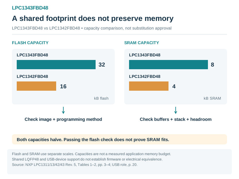
**Figure 1. LPC1343FBD48 USB diagnostic stages.** Engineering diagnostic sequence synthesized from NXP’s LPC1343FBD48 guidance. CPU startup, USB attachment, enumeration and application transfer are separate observations. Check the installed revision’s errata and retain the first failing stage; this is a proposed method, not a report of board tests. Sources: [supporting source 1](https://www.nxp.com/docs/en/data-sheet/LPC1311_13_42_43.pdf); [supporting source 2](https://www.nxp.com/docs/en/errata/ES_LPC134X.pdf). **Figure 2. LPC1343FBD48 to LPC1342FBD48 memory-capacity screening.** Manufacturer capacity comparison with two separate scales: flash and SRAM. The related LPC1342FBD48 provides half the flash and half the SRAM of LPC1343FBD48 despite the shared LQFP48 outline and USB-device role. Check the complete programming image separately from buffers, stack and runtime headroom. No actual firmware size, runtime margin, current availability or drop-in compatibility is established. Sources: [supporting source 1](https://www.nxp.com/docs/en/data-sheet/LPC1311_13_42_43.pdf).Before changing components, assemble a reproducible baseline: PCB revision, populated BOM, device marking, firmware image and source revision, compiler configuration, USB descriptors, host operating system, cable, and whether power comes from USB or an independent supply. Preserve a known-good board if one exists. Comparing two boards with different firmware and different cables can make a simple fault look intermittent.
Separate three questions in the test log. Does the MCU start? Does the host detect a USB attachment and complete enumeration? Does the application exchange the intended data afterward? A passing answer to one question does not prove the next. Keeping those boundaries visible narrows the next measurement.
The general device supply range is 2.0–3.6 V, but the USB function requires 3.0–3.6 V. This distinction is explicit in the static-characteristics footnotes. A board that executes code below 3.0 V has not demonstrated valid USB operation. Measure VDD at both supply pins during attachment, reset, enumeration, and the application's load changes. Include regulator tolerance, cable drop, and the actual ground reference. NXP datasheet, Table 7 and footnote 2, pp. 32–35.
Do not use the datasheet's typical active current as a complete board power budget. Its measurement disables peripherals and defines particular pin states and clock sources. USB, the oscillator, application peripherals, and external loads change the total. Likewise, the deep-power-down figure does not represent a USB-connected device maintaining its communications state. The power-mode descriptions and current-test conditions need to travel with any number used in a design review. NXP datasheet, pp. 27–28 and 32–46.
An existing self-powered product needs a deliberate cable-disconnect test. Measure the board with its own supply on and USB absent, then with USB present while the local supply is off. Look for unintended powering through signal or sense paths. The datasheet's 5 V tolerance for relevant digital pins is conditional on VDD being present; USB D+ and D− are not 5 V-tolerant pads. A “5 V tolerant” label applied to the MCU as a whole is therefore misleading. NXP datasheet, pin-table footnotes and input conditions, pp. 13 and 31–35.
After reset, LPC1343 starts from its internal RC oscillator. That makes basic CPU execution possible before the external oscillator is ready. USB is different: NXP requires the system oscillator as the source for USB, with a dedicated USB PLL available to generate the 48 MHz clock. A running LED demonstration proves little about this clock path. NXP datasheet, clock diagram and Sections 7.18.1–7.18.2, pp. 24–26.
Audit the startup code against the populated oscillator. Record the actual crystal or external clock frequency, source selection, PLL settings, lock indication, USB clock divider, and clock-enable sequence. Verify that the code waits for the required stabilization before the USB peripheral is used. Avoid carrying oscillator constants from an evaluation board into a repaired production board without comparing their BOMs.
A useful diagnostic firmware build exposes a suitable divided clock on CLKOUT when the board's pin use permits it. Treat that as an intentional diagnostic configuration: PIO0_1 also has boot-related behavior and other multiplexed functions, so the measurement must not change the starting conditions being investigated. Read back the configuration as well as measuring the output. A clock on a pin confirms the selected route to that pin, not automatically every internal USB clock gate.
If the board uses an external oscillator module, check its electrical drive interface. XTALIN is not an ordinary 3.3 V GPIO input. The datasheet's external-clock application guidance limits the oscillator input and describes capacitive coupling and attenuation. If it uses a crystal, compare its load capacitance and series resistance with the specified oscillator mode, fitted capacitors, and PCB parasitics. Substituting “another crystal of the same frequency” can change startup margin. NXP datasheet, pp. 59–61.
For a legacy board that works only after touching a probe to the crystal, avoid treating that observation as a fix. The probe changes loading. Investigate the oscillator network and its startup behavior using a measurement method appropriate to the circuit.
LPC1343 integrates the USB PHY, but the external connection still matters. NXP's suggested circuits show series resistors in D+ and D− and an external 1.5 kΩ pull-up on D+. Its self-powered example uses USB_CONNECT to control a switch in that pull-up path. These are concrete dependencies to inspect on an old board, especially after repair or a BOM substitution. NXP datasheet, Section 11.1, p. 59.
Table 1. USB bring-up nodes for LPC1343FBD48 in LQFP48
| Node | Physical pin(s) | What to verify on the assembled board |
|---|---|---|
| VDD / VSS | VDD 8, 44; VSS 5, 41 | Correct supply and return at the MCU; USB operation stays within 3.0–3.6 V |
| USB_DM / USB_DP | 19 / 20 | Correct connector polarity, continuity, fitted series resistors, no solder bridge |
| USB_VBUS / PIO0_3 | 14 | Actual cable-power sensing and its reset-time role; no assumed powered-off tolerance |
| USB_CONNECT / PIO0_6 | 22 | Correct pin function and external attach-switch behavior where used |
| XTALIN / XTALOUT | 6 / 7 | Populated oscillator matches firmware and electrical interface requirements |
| RESET / PIO0_0 | 3 | Valid reset behavior and no unintentional external loading |
| PIO0_1 | 4 | Reset-time boot request state is intentional |
| SWCLK / SWDIO | 29 / 39 | Debug access remains available in the chosen pin and protection configuration |
Source: NXP datasheet, LQFP48 pin diagram and Table 3, pp. 6 and 10–13. Compiled by YG Group; these pin numbers do not apply to HVQFN33.
The electrical-characteristics table specifies the USB output impedance with external 33 Ω ±1% series resistors included. Do not read that impedance as a property of the bare IC and then add a second unrelated termination assumption. Check the board's fitted values and the placement relative to the original qualified design. NXP datasheet, Table 7 footnote 18, p. 35.
If a protection component or connector has changed, continuity is only the first check. Review the altered capacitance, return path, and differential routing, then validate the signal on the assembled board. A basic enumeration pass is useful evidence, but it is not equivalent to USB electrical compliance testing over the product's operating conditions.
NXP's bus-powered and self-powered drawings are interface suggestions rather than complete product power architectures. In particular, the MCU's VDD must not be confused with the connector's nominal USB bus power. Retain the product's appropriate supply regulation and power-path design.
PIO0_1 and PIO0_3 influence the boot path. With the relevant ISP request at reset, PIO0_3 selects between UART ISP and USB device enumeration. In an assembled product, a peripheral or test fixture connected to either pin can therefore change what runs before the application begins. Scope those levels through reset instead of relying only on the schematic's resistor labels. NXP datasheet, Table 3 and boot-loader description, pp. 10 and 29.
Use the ROM path as a separate diagnostic case, not as proof that the application descriptors and endpoint service code are correct. Conversely, an application that enumerates does not demonstrate that the factory recovery procedure remains usable. Record the intended path, host-visible identity, firmware state, and result for each test.
The device is a USB device controller. It does not become a USB host simply because the ROM supports mass-storage-related programming. Connecting a USB flash drive to a passive connector arrangement does not create a supported host architecture. Keep the role of the external host explicit when documenting the service procedure. NXP datasheet, Section 7.9, p. 20.
NXP's applicable errata adds four checks: VDD.1 changes the power-ramp starting limit to 200 mV or below; ISP.2 identifies unreliable power-up USB ISP enumeration with bootloader 5.2 and lists no workaround; USB.1 requires the control-status packet before the bulk CSW in the described recovery sequence; ISP.1 flags CRP1/CRP2 behavior in USB ISP. Match these to the installed revision and service workflow. NXP ES_LPC134X, Rev. 6.2, pp. 3 and 7–10.
Do not turn a debugging experiment into an irreversible production change. Preserve the approved programming image and its recovery policy. In particular, changes to code protection or permanent sector locking require an engineering plan for future servicing; they are not routine fixes for a board that temporarily disappears from a host.
A practical investigation moves from physical evidence toward software state. Start with the device's supply, reset, and oscillator; then inspect attachment; then capture the host's enumeration traffic; finally exercise the application's transfers. Change one variable at a time and retain the last passing configuration.
Table 2. A symptom-driven investigation sequence
| Observation | First discriminating check | Evidence to save |
|---|---|---|
| MCU does not start reliably | Supply waveform, complete power-down, reset state, and applicable power-up errata | VDD/reset captures and the exact power sequence |
| MCU runs, but host sees no attachment | D+ pull-up path, USB_CONNECT state, connector continuity, VBUS detection | Pin states and connector-to-MCU checks |
| Host detects attachment but enumeration fails | USB clock route, reset events, control-transfer log, boot mode | Clock configuration and host trace |
| ROM test works but application fails | Application initialization, descriptors, endpoint mapping, interrupt service | Firmware revision, descriptor dump, first failing transaction |
| Transfer fails after a recovery or clear-halt event | Class-specific endpoint handling and applicable USB errata | Reproducible command sequence and bus trace |
| Failure follows a repair or BOM change | Actual fitted oscillator, series resistors, protection, and assembly | Before/after BOM and inspection record |
Source: engineering diagnostic workflow compiled by YG Group using the NXP datasheet. Symptoms narrow the investigation; they do not establish a fault without measurement.
For application enumeration, compare the host's first failed request with the firmware's actual state. Verify that the declared interfaces and endpoints match what the software initializes, and that request handling does not depend on a debugger pausing execution. Test with the debugger detached, because timing and reset behavior during a debug session can differ from the production startup path.
The endpoint configuration is not an arbitrary pool. NXP identifies control, interrupt/bulk, and isochronous endpoint roles, with buffering distinctions. Use the table for the actual endpoint allocation rather than copying a descriptor layout from another LPC family. For the ordinary control and interrupt/bulk entries, Table 5 specifies 64-byte packets; bulk double buffering is available on the listed endpoint pair. This does not make 12 Mbit/s a guaranteed application payload rate. Host scheduling, class protocol, software service time, and packet overhead remain relevant. NXP datasheet, Table 5, p. 20.
The same page's general buffer-size bullet and its isochronous row are not worded consistently. This guide does not use the isochronous value to size a design. A maintenance task that depends on isochronous buffering should resolve the detailed behavior against the relevant user manual and software implementation before changing descriptors or buffers.
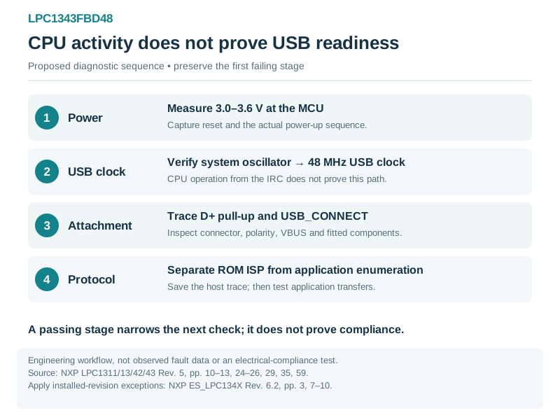
LPC1343FBD48 provides 32 kB flash and 8 kB SRAM. A maintenance build can exceed those limits even when the original binary fitted: compiler changes, diagnostics, additional descriptors, buffering, and stack growth all consume space. Review the linker map and measured worst-case stack behavior appropriate to the application. Leave room for the service features the product actually needs rather than equating a successful link with a safe runtime memory budget.
LPC1342FBD48 is the closest related device in this article's selected pair. It uses the same LQFP48 package and is listed with USB device support, but only 16 kB flash and 4 kB SRAM. It should not be approved as a purchasing replacement merely because the footprint matches. NXP datasheet, Tables 1–2, pp. 3–4.
Table 3. What the related-device comparison does—and does not—establish
| Item | LPC1343FBD48 | LPC1342FBD48 | Maintenance decision |
|---|---|---|---|
| Package | LQFP48, SOT313-2 | LQFP48, SOT313-2 | Shared outline is a starting point for review |
| Flash | 32 kB | 16 kB | Rebuild and inspect the complete image and programming method |
| SRAM | 8 kB | 4 kB | Re-evaluate buffers, stack, and runtime headroom |
| USB role | Full-speed device | Full-speed device | Same role does not prove binary or application equivalence |
| Qualification | Exact existing design must be known | Requires project-specific validation | No unrestricted drop-in claim is made |
Source: NXP datasheet, pp. 3–4 and 20. Compiled by YG Group. This table does not establish current availability of either device.
Do not transfer the LPC1300L low-current profiles, extra SSP controller, or windowed watchdog features to LPC1343 simply because they appear in the same PDF. Those enhancements are identified for different variants. A feature checklist should be built from the exact row and its footnotes.
A repaired board should be tested through the conditions that originally exposed the problem, including cold start, repeated cable attachment, application reset, and the product's intended suspend or recovery behavior. Define the relevant host and cable set from actual deployment needs.
Retain enough information to reproduce a failure: full device identity, board and firmware revisions, fitted clock parts, power source, host trace, and the first failed stage. Record whether each observation is a measured result, a datasheet limit, or an engineering hypothesis. If the conclusion is “the PCB is correct,” it should be supported by the particular interfaces checked, not by one successful enumeration event.
For a release, keep the programming and recovery procedure with the same configuration record. Production and service teams need to know which image to use, how the boot pins are driven, what the expected host-visible device is, and what to do when the prescribed procedure fails. This prevents a future technician from treating a ROM limitation as a reason to modify otherwise working USB hardware.
For LPC1343FBD48 maintenance, a useful bring-up sequence proves power, clock, attachment, boot path, and application behavior separately. Apply the correct USB voltage range, inspect the external interface components, and review the relevant errata before changing the PCB. Once the failing stage is reproducible, make the smallest justified change and retain the evidence with the board and firmware revisions. The result is a serviceable legacy configuration with clear limits.