
Veca Huang




| Picture | Part Number | Manufacturer | Stock | Action |
|---|---|---|---|---|
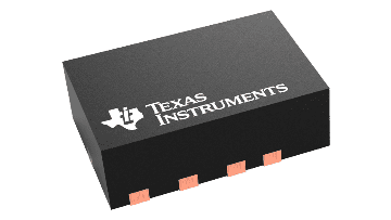 | LMR36015ARNXR | Texas Instruments | 6,590 | |
| LMR36015BRNXR | Texas Instruments | 4,680 | |
| LMR36015FBRNXR | Texas Instruments | 8,030 | |
| LMR36006BRNXR | Texas Instruments | 8,380 | |
| LMR33620ARNXR | Texas Instruments | 6,840 |
No. TI identifies LMR36015ARNXR as the adjustable 400 kHz version without forced PWM. It can change to pulse-frequency modulation at light load. Record load current when comparing switching and ripple waveforms; a change in pulse pattern can be normal operating behavior. The similarly named FBRNXR version has a different switching-mode selection and must not supply the mode assumptions for ARNXR.
Place the small local bypass capacitors at both VIN/PGND pairs before routing less critical connections. TI illustrates two 220 nF high-frequency capacitors alongside the larger input capacitance and calls for at least 4.7 µF effective ceramic input capacitance. Effective capacitance means the value available under operating bias and temperature, not simply the nominal value printed in the bill of materials.
Fast switching current completes a loop through the input capacitor and power switches. Inductance anywhere in that loop can produce voltage during a current edge. A short VIN trace combined with a long PGND return can therefore remain problematic. Review vias, reference planes and any plane interruptions when judging the complete connection.
Category: Manufacturer Insights
Author: Veca Huang
The LMR36015ARNXR is a 60 V, 1.5 A synchronous buck converter, but those ratings do not describe the electrical behavior of the copper around it. Its input capacitors, two VIN connections, two PGND connections and internal switches form a fast current loop. A filter at the power connector can reduce noise leaving the board; it cannot remove the inductance already inside that switching loop.
For this exact ordering code, start with the 400 kHz automatic PWM/PFM configuration, then place the local input capacitors around the RNX package before routing the remaining power stage. The practical objective is to keep switching current local, give it a closely coupled return, and prevent the feedback circuit from measuring switching interference. This article follows the supplied TI LMR36015 datasheet, SNVSB49D, including its application examples and ordering information. Calculated examples below illustrate layout sensitivity; they are not measurements of a finished board.
LMR36015 is a family name. The characters between that name and the reel suffix distinguish operating behavior that matters when interpreting a waveform. TI's device comparison table identifies LMR36015ARNXR as an adjustable-output, 400 kHz part without forced PWM. It identifies the B version as a 1 MHz alternative, while the FB version includes forced PWM. A layout review that treats all three as the same device can misdiagnose a normal light-load waveform as instability.
Not necessarily. A compact local loop reduces an important noise source, while an input filter addresses the noise path through the supply network. TI’s EMI examples use defined operating and test conditions. The finished board, cables and enclosure still require evaluation. Adding a filter also creates source-impedance and resonance questions that should be checked during startup and load changes.
TI describes VCC as the internal regulator output and calls for local bypassing. It is not a general external power supply. Follow the stated permitted use, including the documented power-good pullup case, instead of attaching unrelated loads. Extra loading can change the assumptions behind startup and internal supply operation.
A similar package name is insufficient. Compare exact pin functions, input-voltage range, switching frequency, operating mode, current capability and recommended external components. LMR33620ARNXR, for example, has a lower input-voltage range despite its higher current capability. A replacement requires a complete application review and validation on the intended board.
At sufficient load, the ARNXR operates with regular PWM switching. At light load it can enter pulse-frequency modulation, reducing switching activity to improve efficiency. The switching intervals and output ripple pattern can therefore change with load. A screenshot taken at a few milliamperes and another taken at full load answer different questions. Record the operating point alongside the waveform before deciding that a different input filter or compensation component is needed.
The recommended input range is 4.2 V to 60 V. The absolute maximum input rating is a separate stress boundary, not extra continuous operating headroom. A nominal industrial supply may remain comfortably below 60 V while cable connection or load disconnection produces a higher local peak. That peak must be evaluated at the converter pins. The voltage printed on the system power supply is not a substitute for that measurement.
Table 1. Exact-device facts that change the layout review
| Item | LMR36015ARNXR evidence | Consequence for the board |
|---|---|---|
| Switching selection | Adjustable output, 400 kHz, no forced PWM | Include light-load PFM when interpreting ripple |
| Recommended input | 4.2 V to 60 V | Check the local rail across normal operating conditions |
| Output current | Up to 1.5 A under applicable operating conditions | Verify current, temperature and component limits together |
| Package | Twelve-pin RNX VQFN-HR, nominal 2 mm by 3 mm | Use the exact land pattern and pin map |
| Power connections | Two VIN pins and two PGND pins | Place bypass paths on both sides of the package |
| Feedback reference | Nominal 1 V | Keep the divider return and feedback trace electrically quiet |
The small package does not make component placement optional. Its arrangement is intended to support short, balanced input-current paths. Routing both VIN pins through a long narrow neck before reaching one remote capacitor defeats much of that opportunity. Likewise, connecting both PGND pins through a distant via cluster creates shared impedance where the layout most needs a local return.
A buck converter has several current paths, but not all of them change equally fast. The inductor current changes comparatively gradually during a switching cycle. The input current of the switching stage changes sharply as the high-side switch turns on and off. The difference between the two switch states identifies the high-frequency loop: local input capacitor, high-side switch, low-side switch and return to the input capacitor.
This distinction changes how “close” should be judged. A capacitor may look close to the IC in a top-side rendering while its ground terminal connects through a long path on another layer. The relevant distance is the complete electrical loop, including vias, plane transitions and the connection between the capacitor return and PGND. Measure proximity along that path, not only between component centers.
Inductance produces a voltage according to V = L × di/dt. For an illustrative current change of 1 A in 5 ns, a 1 nH loop contributes 0.2 V and a 5 nH loop contributes 1 V. These values are a sensitivity calculation, not an estimate of the LMR36015's actual current edge. The useful conclusion is that reducing a few nanohenries can matter even when the DC resistance of the copper appears negligible.
The loop also couples energy into nearby structures. A larger loop presents more magnetic area, while the switch node couples through electric fields to neighboring copper. These mechanisms are related but should not be treated as one problem. Reducing the input loop area addresses a switching-current source. Reducing unnecessary SW copper and separating sensitive nets addresses another coupling path. A design can improve one while making the other worse.

Figure 1. Conceptual switching-current loop. The drawing emphasizes the complete capacitor-to-switch return path; it is not an RNX footprint or a production routing file.
Review the routing in three dimensions. A continuous ground plane close to the top layer can provide a short return path and useful shielding. However, a split or slot under the relevant connection can force current around an obstacle. A via close to a capacitor is helpful only if it connects to the intended plane and that plane connects back without a large detour. The stackup belongs in the layout review, not in a separate mechanical appendix.
TI's application guidance calls for at least 4.7 µF of effective ceramic input capacitance and illustrates small high-frequency capacitors at the two VIN/PGND pairs. Its design example uses two 220 nF capacitors in addition to the larger input capacitance. “Effective” matters: the value available at operating DC voltage and temperature can be lower than the nominal capacitance on a purchasing line.
Place each small bypass capacitor so its terminals connect directly into the adjacent VIN and PGND path. Short, broad copper is generally preferable to a narrow track that meanders around a test point. Keep the two paths reasonably balanced where the routing permits. The aim is to make both sides useful at high frequency, not to produce a visually symmetric drawing at the expense of electrical continuity.
The larger ceramic input capacitor should remain close enough to supply the switching stage without relying on a long supply trace. Bulk capacitance farther upstream serves a different time scale. It may help with cable connection, source impedance or slower load changes, but its distance and parasitics can prevent it from replacing the small local capacitors during a fast switching edge.
Voltage rating needs a separate check from capacitance. TI recommends selecting the input capacitor rating above the maximum input voltage, preferably with additional margin, and illustrates a high-voltage X7R selection. Do not assume that any capacitor marked 4.7 µF maintains that value near a 60 V rail. Consult its exact manufacturer's bias data, package and temperature characteristics before treating it as the minimum effective capacitance.
Table 2. Placement order for a defensible first layout
| Order | Component or connection | Placement objective | Review question |
|---|---|---|---|
| First | Small capacitors at both VIN/PGND pairs | Contain fast input-current changes | Does each return reach its PGND without a long detour? |
| Second | Main ceramic input capacitor | Supply local switching energy | Is effective capacitance sufficient at maximum input? |
| Third | Inductor and output capacitors | Keep the power path short | Is SW copper limited to what routing and heat require? |
| Fourth | Bootstrap and VCC capacitors | Keep internal supply loops compact | Are their required nodes connected directly? |
| Fifth | Divider and feedback connection | Sense the intended output voltage | Is FB separated from the switching power paths? |
Input-capacitor RMS current is also relevant. A simple buck estimate places the worst input RMS current near half the output current, although the actual duty cycle and ripple must be included in a final calculation. Capacitance alone does not establish adequate ripple-current performance. Heating, dielectric behavior and the permitted operating envelope still belong in the component review.
Do not route a convenient supply test point through the narrow space needed by these capacitors. A test feature is useful when it supports an accurate measurement without compromising the circuit being measured. Where space is tight, provide a dedicated probe location outside the critical local connection rather than inserting a long branch into the hot loop.
SW is a high-dv/dt node. Its copper connects the switching output to the inductor and also participates in the bootstrap connection. Extra copper can increase capacitive coupling to other layers and traces. Expanding SW into a broad polygon merely because it carries current can therefore create a noise source that a connector filter does little to address.
Use enough copper for the electrical and thermal requirement, then stop. The useful review question is whether each extension of the SW area has a purpose. A long spur to a distant probe pad, a large unused pour beneath a signal region or an unnecessary layer change adds parasitics without helping the primary current path. If a probe point is required, keep its access short and account for the probe capacitance during testing.
The datasheet's pin description includes a deliberate connection from SW to the NC pin to simplify the bootstrap-capacitor route. That NC pin has no internal connection, but the application routing uses it as a convenient external node. A library rule that automatically prohibits all copper on every pin called NC can therefore conflict with this particular device's recommended implementation. Read the exact pin description before applying a generic convention.
The bootstrap capacitor is 100 nF in TI's guidance and connects between BOOT and SW. Its loop should be compact. The VCC capacitor serves a different function: it bypasses the internal regulator output to ground. TI calls for a 1 µF capacitor there and cautions against using VCC to power unrelated external loads. A local logic circuit attached to VCC can change startup and loading assumptions that the buck design never intended to support.
There is also a thermal tradeoff. The RNX implementation does not provide an exposed die-attach pad that can simply be copied from a larger regulator footprint. Heat spreads through the package connections and surrounding board. TI's layout uses substantial ground copper and thermal connections while keeping the sensitive electrical loops controlled. A small SW region and an adequate thermal design are compatible when the ground and power copper are planned deliberately.
The feedback divider is the converter's measurement circuit. If switching current shares impedance with its reference, the controller can respond to a voltage disturbance that is not representative of the intended output. A filter added at the input connector will not necessarily fix that local sensing error.
Place the divider close to FB and route the feedback connection away from the inductor, SW copper and input switching loop. Take the output sense from a suitable quiet point at the output capacitor region. The bottom of the divider should reference the intended analog ground path rather than a piece of copper carrying a large pulsed return current. At the same time, AGND and PGND must be connected in accordance with TI's layout guidance; leaving them as unrelated isolated islands is not an improvement.
A ground plane is useful because it provides a broad low-impedance reference. It is not a license to ignore where current enters and leaves the plane. If a high-current return must cross the narrow neck beneath the divider, the nominal net name GND hides the physical problem. Inspect current flow and copper geometry together when deciding where to place vias and how to join the local ground regions.
The power-good output is open drain and requires an appropriate pullup when used. The enable pin must not float. These control connections should be checked while reviewing feedback because they can create symptoms that resemble power-stage problems. An unstable enable voltage can repeatedly restart a converter with an otherwise acceptable layout; an incorrectly loaded power-good connection can mislead system firmware without changing output regulation.
Table 3. Symptoms and the next discriminating observation
| Observation | Possible layout or operating cause | Useful next check |
|---|---|---|
| Large edge-related spikes at VIN | Local input-loop inductance or probing loop | Reprobe directly across local bypass terminals |
| Ripple changes markedly at light load | Normal automatic PWM/PFM transition | Compare load and switching activity with the exact ARNXR mode |
| Output disturbance coincides with SW edges | Coupling into feedback or output measurement | Inspect FB routing and use a short output probe return |
| Input oscillation after adding a filter | Source/filter interaction or inadequate damping | Measure both sides of the filter during startup and load changes |
| High package temperature | Board thermal path or excess loss | Measure operating conditions and review copper against the thermal model |
These observations are not fault diagnoses by themselves. For example, output spikes may be real differential ripple, common-mode pickup or the result of a long oscilloscope ground lead. A useful troubleshooting sequence changes one measurement condition or layout hypothesis at a time, preserving enough information to explain why a symptom changed.
Figure 2 plots V = L × di/dt for several assumed current slew rates. It isolates one relationship so that the effect of loop inductance is visible. The plot does not include package inductance, nonlinear capacitance, damping, switch timing or the resonant network of a real board. It should guide placement priorities, not be pasted into a component qualification report as predicted overshoot.
For example, if a layout change shortens both the VIN route and its return, it may reduce loop inductance. The plot explains why that is worth investigating. It does not determine the improvement in decibels or prove that a particular emission peak will disappear. A simulation with credible parasitics or a controlled measurement is needed for those claims.

Figure 2. Calculated inductive voltage from V = L × di/dt. All slew rates and inductances are illustrative inputs, not extracted LMR36015ARNXR measurements.
Use the same discipline when reading TI's EMI plots. The supplied examples specify an input of 13.5 V, a 5 V output and a 1.5 A load, along with a particular board and filter arrangement. Those results are valuable evidence that the implementation can perform well under the stated setup. They do not certify a different enclosure, cable harness, grounding arrangement or operating voltage.
When evaluating two placements, keep the power-stage values and operating point unchanged for the first comparison. Changing the inductor, switching version and capacitor location together makes it difficult to identify why ringing or emissions changed. A controlled comparison can begin with the same schematic and a deliberately shorter pair of input bypass connections.
Document both the forward and return geometry in the comparison. A shorter VIN trace may appear to be the improvement while an unnoticed ground-plane change is actually responsible. Conversely, a visually cleaner placement can perform worse if it inserts a via transition into a previously direct local loop. Screenshots of the relevant layers help preserve that distinction for review.
Use consistent probing, cable placement and load conditions. If the goal is to compare high-frequency edge behavior, a change in probe return length can be larger than the effect being investigated. If the goal is conducted emissions, a different supply lead arrangement can alter the network. Reproducibility gives the team confidence that a chosen layout change addresses the circuit rather than the test fixture.
A filter is a legitimate design element. The title's placement priority does not imply that a converter should never need one. It means that the filter should solve an identified conducted-noise problem after the local switching structure is sound. Otherwise, more components can conceal the original cause while introducing new resonances, losses or startup behavior.
Begin by identifying where the unwanted energy travels. Differential-mode noise between supply and return calls for a different interpretation than common-mode current involving the enclosure or cable environment. A layout change that reduces a local radiating loop may improve a radiated result without substantially changing a conducted result. Conversely, an input filter may reduce conducted noise while leaving a large SW electric-field source near a sensitive interface.
Long supply leads and low-ESR ceramic capacitors can form an underdamped input network. The datasheet discusses this condition and the use of bulk capacitance and damping. Simply selecting a larger ceramic bank may move the resonance rather than remove it. The source impedance, cable inductance, filter impedance and converter behavior need to be considered together.
Check startup, shutdown and rapid supply changes as well as steady operation. A converter with stored output energy can experience a very different current path when its input collapses. TI specifically discusses input protection and the behavior of snapback transient suppressors in such circumstances. Choose protection based on the actual system transient and energy path, not solely on a nominal clamp-voltage number.
The inductor and output capacitors must still be designed for the chosen output, ripple and operating range. TI presents more than one application example, so a value appearing beside one schematic is not a universal bill of materials. Preserve the conditions attached to each example when selecting inductance, saturation current and effective output capacitance. A layout review cannot rescue a component set that is outside the converter's documented design guidance.
The four devices below are useful comparison candidates for a new design or a redesign. They are not approved substitutions. Two change behavior within the LMR36015 family; the others change current or voltage capability. Their value is in showing which requirement needs to be revisited when a purchasing or design team proposes another part.
Table 4. Four related orderable models and their review boundaries
| Exact model | Relationship to LMR36015ARNXR | Why consider it | What must be rechecked |
|---|---|---|---|
| LMR36015BRNXR | Same family, 1 MHz automatic operating version | Different switching-frequency and component tradeoff | Inductor, capacitor, loss and EMI behavior |
| LMR36015FBRNXR | Same family, 1 MHz forced-PWM version | Applications needing a different light-load switching policy | Light-load loss, ripple and complete power-stage design |
| LMR36006BRNXR | Related 60 V, 0.6 A buck family | Lower-output-current requirement | Exact frequency, pin functions, current margin and application circuit |
| LMR33620ARNXR | Related 36 V, 2 A buck device | More current on a lower-voltage input system | Maximum input and transients, package details, thermal and component selection |
TI's exact-part and family resources support these identities. Matching RNX letters does not establish that the existing board is ready for another device. A reviewer should compare the pin-function table, enable thresholds, control behavior and component recommendations, even when a mechanical footprint appears familiar. Differences in switching frequency can change both required energy storage and the frequency range in which a layout defect becomes visible.
The 36 V candidate is particularly useful as a boundary example. Its higher output-current headline does not make it an upgrade for a rail that needs the LMR36015's 60 V input range. Selection is a set of simultaneous constraints, not a ranking based on one large number. Rejecting an unsuitable candidate early is often more valuable than trying to characterize it on a board for which it was never intended.
Before fabrication, trace the two local input bypass loops in the CAD tool. Hide unrelated layers, then restore them to inspect return planes and transitions. Follow VIN into each capacitor and the converter, then follow PGND back. Next, inspect SW, the inductor and output capacitors. Only after those paths are clear should the reviewer focus on the divider, enable, power-good and measurement access.
During bring-up, record supply voltage at the board connector and at the local input capacitor. Use a suitable short-return probing method for switching edges, and document bandwidth settings. Record output load and temperature. Compare a representative light-load point with a heavier-load point so the normal operating-mode change is visible. This prevents a misleading comparison between two waveforms captured under different conditions.
Thermal measurements should identify ambient conditions, airflow, board orientation and the location being measured. The datasheet's junction-to-ambient figure is tied to a standardized board condition; it is not a fixed property of every finished PCB. A board with less copper, different layer construction or restricted airflow can run hotter at the same electrical load. If the temperature is unexpected, inspect losses and the thermal path together.
Table 5. Evidence to retain before releasing the layout
| Review stage | Record to retain | Decision supported |
|---|---|---|
| Identity | Exact ARNXR code, datasheet revision and pin map | Correct switching version and footprint |
| Placement | Annotated VIN/PGND loops and capacitor part numbers | Local loop and effective-capacitance review |
| Signal integrity | FB route, return connection and probe method | Separation of sensing error from actual ripple |
| Power and temperature | Input range, load sweep and measured thermal conditions | Operating margin under the intended use |
| EMI and source behavior | Test arrangement, cables, filter and startup waveforms | Whether the remaining filter addresses the observed path |
A good release record explains the relationship between the schematic, the copper and the measured result. It does not merely show that the converter produced the right output once. For LMR36015ARNXR, the strongest starting point is a compact, deliberate input-current loop on both sides of the package. The filter decision then becomes a response to evidence from the complete board, with its operating mode, source and measurement conditions explicitly understood.