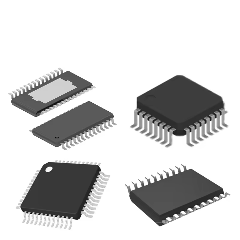
The AD9699 is a single, 14-bit, 3 GSPS analog-to-digital converter (ADC). The device has an on-chip buffer and a sample-and-hold circuit designed for low power, small size, and ease of use. This product is designed to support applications capable of direct sampling wide bandwidth analog signals of up to 5 GHz. The −3 dB bandwidth of the ADC input is 9 GHz. The AD9699 is optimized for wide input bandwidth, high sampling rate, excellent linearity, and low power in a small package.The ADC core features a multistage, differential pipelined architecture with integrated output error correction logic. The ADC features wide bandwidth inputs supporting a variety of user-selectable input ranges. An integrated voltage reference eases design considerations. The analog input and clock signals are differential inputs. The ADC data outputs are internally connected to four digital down-converters (DDCs) through a crossbar multiplexer (mux). Each DDC consists of up to five cascaded signal processing stages: a 48-bit frequency translator (numerically controlled oscillator (NCO)), and up to four half-band decimation filters. The NCO has the option to select preset bands over the general-purpose input/output (GPIO) pins, which enables the selection of up to three bands. Operation of the AD9699 between the DDC modes is selectable via serial peripheral interface (SPI)-programmable profiles.In addition to the DDC blocks, the AD9699 has several functions that simplify the automatic gain control (AGC) function in a communications receiver. The programmable threshold detector allows monitoring of the incoming signal power using the fast detect control bits in Register 0x0245 of the ADC. If the input signal level exceeds the programmable threshold, the fast detect indicator goes high. Because this threshold indicator has low latency, the user can quickly turn down the system gain to avoid an overrange condition at the ADC input. In addition to the fast detect outputs, the AD9699 also offers signal monitoring capability. The signal monitoring block provides additional information about the signal being digitized by the ADC.The user can configure the Subclass 1 JESD204B-based high speed serialized output in a variety of one-lane, two-lane, four-lane, and eight-lane configurations, depending on the DDC configuration and the acceptable lane rate of the receiving logic device. Multi-device synchronization is supported through the SYSREF± and SYNCINB± input pins.The AD9699 has flexible power-down options that allow significant power savings when desired. All of these features can be program-med using a 3-wire SPI.The AD9699 is available in a Pb-free, 12 mm × 12 mm, 196-ball BGA and is specified over the −40°C to +85°C ambient temperature range. This product is protected by a U.S. patent.Note that throughout the data sheet, multifunction pins, such as FD/GPIO_A0, are referred to either by the entire pin name or by a single function of the pin, for example, FD, when only that function is relevant.PRODUCT HIGHLIGHTS
YG GROUP (YUGUANG INTERNATIONAL(HK)CO.,LTD) supports reliable sourcing through quality controls and compliance documentation. Please confirm product requirements, applicable certifications and supporting documents before ordering.
AD9699 is an authentic electronic component manufactured by Analog Devices, categorized under Data Converter ICs. It is supplied in the standard manufacturer-specified package footprint, providing industry-standard mechanical dimensions and terminal configurations for board-level assembly. Full pinout configurations, physical footprint drawings, and rated operating tolerances are documented in the official AD9699 datasheet above.
Electronic component spot-market pricing for AD9699 fluctuates based on real-time global availability, production date codes, minimum order quantities (MOQ), and packaging formats (e.g., Reel, Tube, Tray). Using an RFQ ensures you receive accurate, real-time volume pricing tied to verified, traceable inventory rather than stale catalog estimates.
Lead times for AD9699 depend on whether stock is dispatched from our central hub or regional franchise partners. Ready-to-ship inventory typically leaves the warehouse within 1–3 business days following quality inspection, while factory-direct or back-ordered allocations are confirmed with an estimated ship date upon RFQ reply.
Loading articles…

Loading articles…
Choose TPS53513RVER Eco-mode or FCCM using load noise, idle power and startup settings, with clear ripple calculations and practical measurement checks.
Read more →
Route MT41K256M16TW-107:P DDR3L with clear VREF, VTT and ODT roles, byte-lane timing, continuous return paths and a documented initialization and validation plan.
Read more →
Build a recoverable W25Q128JVSIQ firmware update around page boundaries, erase timing, BUSY/SUS status, power-up rules and a preserved bootable image.
Read more →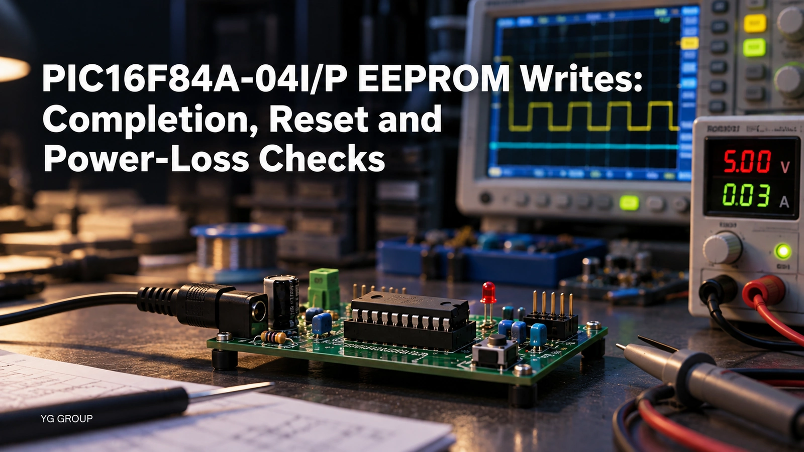
Check PIC16F84A-04I/P EEPROM completion, WRERR reset limits, watchdog timing and two-slot recovery before treating a configuration update as safely saved.
Read more →Loading related products…
| Picture | Part Number | Manufacturer | PDF / RoHS | Stock | Action |
|---|---|---|---|---|---|
| Analog Devices | 8,160 | |||
| Analog Devices | 5,810 | |||
| Analog Devices | -- | 4,540 | ||
| Analog Devices | 7,000 | |||
 | Analog Devices | 6,730 | |||
 | Analog Devices | 7,590 | |||
 | Analog Devices | 5,390 | |||
| Analog Devices | -- | 5,800 | ||
 | Analog Devices | -- | 8,910 | ||
 | Analog Devices | 5,010 |
