
The AD1865 is a complete, dual 18-bit DAC offering excellent THD+N and SNR while requiring no external components. Two complete signal channels are included. This results in cophased voltage or current output signals and eliminates the need for output demultiplexing circuitry. The monolithic AD1865 chip includes CMOS logic elements, bipolar and MOS linear elements and laser-trimmed thin-film resistor elements, all fabricated on Analog Devices' ABCMOS process.The DACs on the AD1865 chip employ a partially segmented architecture. The first four MSBs of each DAC are segmented into 15 elements. The 14 LSBs are produced using standard R-2R techniques. Segment and R-2R resistors are laser trimmed to provide extremely low total harmonic distortion. This architecture minimizes errors at major code transitions resulting in low output glitch and eliminating the need for an external deglitcher. When used in the current output mode, the AD1865 provides two ±1 mA output signals.Each channel is equipped with a high performance output amplifier. These amplifiers achieve fast settling and high slew rate, producing ±3 V signals at load currents up to 8 mA. Each output amplifier is short-circuit protected and can withstand indefinite short circuits to ground.The AD1865 was designed to balance two sets of opposing requirements, channel separation and DAC matching. High channel separation is the result of careful layout. At the same time, both channels of the AD1865 have been designed to ensure matched gain and linearity as well as tracking over time and temperature. This assures optimum performance when used in stereo and multi-DAC per channel applications.A versatile digital interface allows the AD1865 to be directly connected to standard digital filter chips. This interface employs five signals: Data Left (DL), Data Right (DR), Latch Left (LL), Latch Right (LR) and Clock (CLK). DL and DR are the serial input pins for the left and right DAC input registers. Input data bits are clocked into the input register on the rising edge of CLK. A low-going latch edge updates the respective DAC output. For systems using only a single latch signal, LL and LR may be connected together. For systems using only one DATA signal, DR and DL may be connected together.The AD1865 operates with ±5 V power supplies. The digital supply, VL, can be separated from the analog supplies, VSand -VS, for reduced digital feedthrough. Separate analog and digital ground pins are also provided. The AD1865 typically dissipates only 225 mW, with a maximum power dissipation of 260 mW.The AD1865 is packaged in both a 24-pin plastic DIP and a 28-pin SOIC package. Operation is guaranteed over the temperature range of -25°C to +70°C and over the voltage supply range of ±4.75 V to ±5.25 V.
YG GROUP supports reliable sourcing through quality controls and compliance documentation. Please confirm product requirements, applicable certifications and supporting documents before ordering.
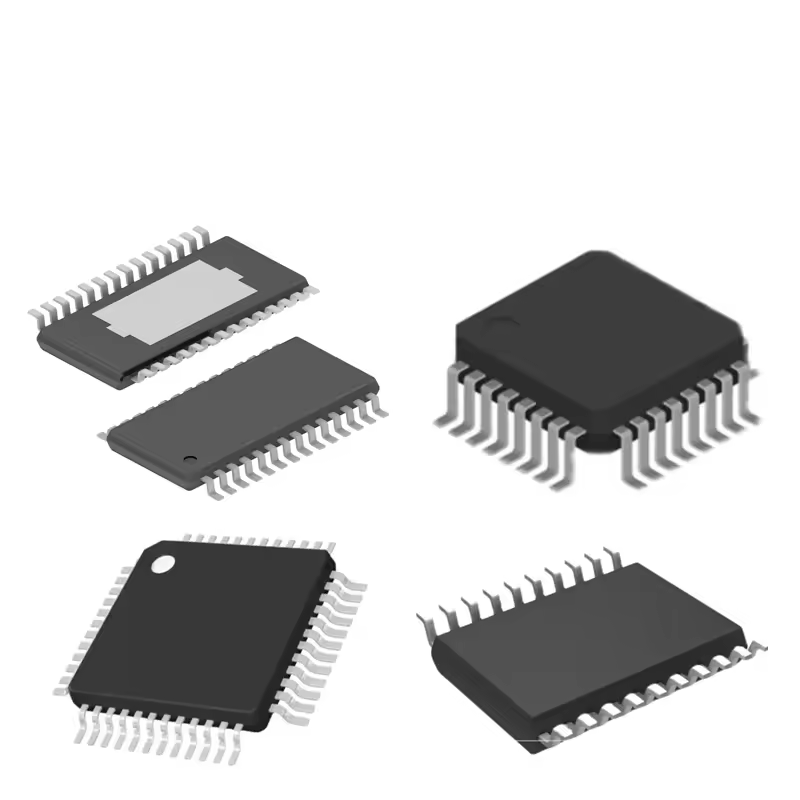
AD1865 is an authentic electronic component manufactured by Analog Devices, categorized under Data Converter ICs. It is supplied in the standard manufacturer-specified package footprint, providing industry-standard mechanical dimensions and terminal configurations for board-level assembly. Full pinout configurations, physical footprint drawings, and rated operating tolerances are documented in the official AD1865 datasheet above.
Electronic component spot-market pricing for AD1865 fluctuates based on real-time global availability, production date codes, minimum order quantities (MOQ), and packaging formats (e.g., Reel, Tube, Tray). Using an RFQ ensures you receive accurate, real-time volume pricing tied to verified, traceable inventory rather than stale catalog estimates.
Lead times for AD1865 depend on whether stock is dispatched from our central hub or regional franchise partners. Ready-to-ship inventory typically leaves the warehouse within 1–3 business days following quality inspection, while factory-direct or back-ordered allocations are confirmed with an estimated ship date upon RFQ reply.
Loading articles…

Loading articles…

Assess LSM6DSV16XTR for robot motion sensing with conditional noise and current figures, OIS range restrictions, FIFO transport calculations and sample-age checks. Compare four related ST sensors without assuming certification or production adoption.
Read more →
Evaluate BTS5030-2EKA for two 12V body-load branches. Review shared thermal loss, lamp inrush, multiplexed diagnosis and the revised 2185 sense ratio without confusing EV forecasts with exact-part demand.
Read more →
Assess what TI's fab expansion means for a TLC555CDR design. Compare exact ordering status, timer behavior and RC tolerance before changing an approved BOM or relying on a delivery promise.
Read more →
Evaluate a DG411AK/883 offer against the circuit it must serve. Compare temperature-dependent leakage, switching behavior, package identity and four nearby models before choosing replenishment or a redesign.
Read more →Loading related products…
| Picture | Part Number | Manufacturer | PDF / RoHS | Stock | Action |
|---|---|---|---|---|---|
 | Analog Devices | 6,790 | |||
 | Analog Devices | 5,280 | |||
 | Analog Devices | 4,580 | |||
| Analog Devices | 1,350 | |||
 | Analog Devices | -- | 3,200 | ||
| Analog Devices | 5,270 | |||
| Analog Devices | 2,770 | |||
 | Analog Devices | 6,420 | |||
 | Analog Devices | - | 5,240 | ||
 | Analog Devices | 7,200 |
