
Scarlett Zhang




| Picture | Part Number | Manufacturer | Stock | Action |
|---|---|---|---|---|
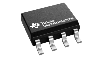 | TLC555CDR | Texas Instruments | 9,980 | |
| NE555DR | Texas Instruments | 2,480 | |
| LMC555CMX/NOPB | Texas Instruments | 8,190 | |
| TLC551CD | Texas Instruments | 8,600 | |
 | TS555IDTTR | STMicroelectronics | 8,800 |
No. TI's December 17, 2025 Sherman announcement establishes a manufacturing event, not a delivery commitment for TLC555CDR. A purchase decision still needs the complete ordering code, required quantity, carrier format and a dated shipment confirmation. If a manufacturing change is claimed to affect your device, request the applicable product evidence. This article has not established that TLC555CDR is manufactured at SM1 or that its price or delivery time has changed because of that fab.
The records reviewed here distinguish them. The September 18, 2026 package addendum and TI's exact ordering page checked on September 23 list TLC555CDR as Active and the TLC555CD tube option as Obsolete. CDR identifies the reviewed tape-and-reel option. Confirm the current full ordering code when buying; do not apply one option's status to the entire TLC555 family. An Active status also does not reserve a quantity or establish a delivery date.
Start with the pinout and electrical conditions, then test the actual circuit. NE555DR, LMC555CMX/NOPB, TLC551CD and TS555IDTTR are comparison candidates in this article, not approved replacements. Review the exact pin assignment, footprint, supply conditions, loaded output levels, reset behavior, timing performance and assembly format. Then test the actual circuit against its requirements. If the replacement needs different timing components, document and approve that circuit change rather than treating the result as a chip-only substitution.
By Scarlett Zhang | YG GROUP
TI's fab expansion is useful context when planning a long-lived product, but a TLC555CDR purchase still depends on the exact orderable device and a dated delivery commitment. This CMOS timer has specific temperature, voltage and timing limits that a factory announcement cannot change. Review the approved BOM, check its timing margin and evaluate a credible alternative before the next urgent order arrives.
When a semiconductor manufacturer opens a fab, buyers have a reasonable question: will the parts on our purchase orders become easier to obtain? That question becomes more useful when attached to a specific device. A mature timer might cost much less than the processor beside it, yet an unapproved substitution can still delay the whole board.
Texas Instruments announced the start of production at its SM1 facility in Sherman, Texas, on December 17, 2025. Its public Sherman page describes a site planned for up to four connected 300mm fabs. These are manufacturer-level facts. The announcement does not identify TLC555CDR as an SM1 product or establish its next delivery date. TI's Sherman manufacturing page and the dated production announcement provide the relevant context.
*Figure 1. Move from manufacturing context to exact-product evidence, board and assembly acceptance, and a dated order commitment. Each step answers a different question. This is an editorial decision flow, not a map of TLC555CDR manufacturing sites. Sources: TI manufacturing, PCN and exact-device information; illustration by YG GROUP.* *Figure 2. Ideal low-frequency RC calculation for RA = 10kΩ, RB = 68kΩ and nominal C = 10nF. The band represents ±1% on both timing resistors while capacitance varies by ±5%. IC error, leakage, temperature effects and parasitics are excluded. This is a calculation, not measured performance or a guaranteed production distribution. Equation basis: TLC555 Rev. K, section 6.3.2; chart by YG GROUP.*For the TLC555C grade, TI's Rev. K recommended operating conditions specify 0°C to 70°C free-air temperature and a 2V to 15V supply. The datasheet's 18V absolute maximum is a stress limit, not a recommended operating voltage. Other grades in the shared document have different temperature and minimum-supply conditions. A commercial CDR device does not inherit their ratings or an automotive qualification from a family-level description.
For the article's illustrative astable circuit, RA = 10kΩ, RB = 68kΩ and C = 10nF give about 988.4Hz using the low-frequency equation. With assumed ±1% resistors and a ±5% capacitor, the passive-only extremes are roughly 932Hz to 1,051Hz. That is a calculation, not a TLC555CDR accuracy guarantee. IC threshold variation, leakage, temperature, parasitics and propagation delay are excluded. Set an application-specific acceptance window and evaluate those additional effects before approving a production design.
Give the complete manufacturer and ordering code, quantity, required carrier, target delivery date and any receiving or traceability requirements. Identify whether this is replenishment of an approved design or a request to evaluate an alternate. For alternatives, include the actual supply, temperature, output load and acceptable timing window so engineering can compare relevant conditions. A general “555 timer” request omits information that can change both the electrical review and the assembler's ability to use the shipment.
For an engineering buyer, the useful response is to separate the planning horizons. A factory investment can inform a conversation about the manufacturer's future footprint. The next board build requires evidence about a particular package, quantity, shipment window and approved source. To connect those two decisions, ask which product information has actually changed.
Keep a proven TLC555CDR design on its approved BOM while reviewing concrete supply evidence. A news-driven substitution creates a new engineering task before it has established a purchasing benefit. Conversely, ignoring all manufacturing changes leaves the team poorly prepared when an affected-product notice or real delivery problem arrives. Use the time before an urgent buy to evaluate a credible fallback while normal purchasing continues.
Table 1 separates the evidence needed for each decision. It is an editorial framework for the buyer, not a description of TI's internal manufacturing sequence.
Table 1. Connect each supply question to evidence at the same level.
| Question | Evidence that can answer it | Useful decision | What remains separate |
|---|---|---|---|
| Has a factory entered production? | Dated manufacturer announcement | Update the supplier's manufacturing context | Whether this timer is made there |
| Does a change affect our device? | Applicable product notice and affected ordering codes | Assess the particular change | Availability of a specific shipment |
| Is the complete device still offered? | Exact ordering page and current status record | Maintain or review the approved orderable code | Price, lot and promised delivery |
| Can our assembly use the supplied format? | Package drawing, carrier details and manufacturing review | Confirm production-line fit | Electrical qualification |
| Can we cover the next build? | Dated quantity and delivery confirmation for the approved item | Schedule the purchase and receiving work | Performance of an untested alternative |
Source: TI's public manufacturing and product-change information; decision framework by YG GROUP.
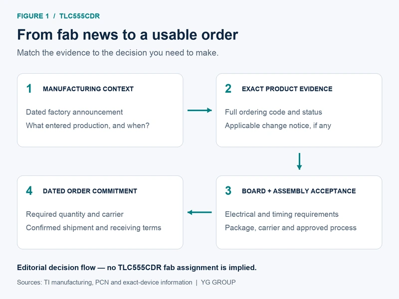
The gap between stages is where purchasing assumptions usually enter. A quote might identify only “TLC555,” while the approved BOM specifies a carrier and temperature grade. A broad availability message might cover a package that the assembler cannot load. Closing those gaps early makes the factory news useful without demanding that it answer questions it never addressed.
TLC555CDR is an eight-pin SOIC device in TI's D package, with a commercial operating-temperature range of 0°C to 70°C. The supplied Rev. K datasheet's September 18, 2026 package addendum lists a standard quantity of 2,500 in large tape and reel. It marks TLC555CDR Active while marking the tube-format TLC555CD Obsolete. The exact TI ordering page, checked on September 23, 2026, shows the same status distinction.
That is a more actionable finding than a general statement about the timer family. A historical BOM that names the tube version needs a different purchasing review from one already specifying the reel. The logic function may be familiar to the design team, but the assembler still needs the correct feeder format, orientation and receiving record.
The status distinction also gives the headline a practical limit: even within one established device family, orderable options can have different lifecycle records. Broad manufacturing investment cannot be substituted for that record. Equally, an Active label does not reserve stock or fix a lead time. Record the status as a dated observation and obtain the commercial commitment separately.
Preserve the full TLC555CDR identity through the quote, order and receiving record. A shorthand family name is convenient in conversation; it is weak identification for a shipment that must match an approved assembly process.
Table 2. What the TLC555CDR identity means for this BOM.
| Item | Confirmed baseline | Practical implication |
|---|---|---|
| Manufacturer and ordering code | Texas Instruments, TLC555CDR | Match the complete code on purchasing documents |
| Electrical family | Single CMOS timer | Review the actual timing and output circuit, not just “555” in a description |
| Package | D, eight-pin SOIC | Check the released land pattern and assembly program |
| Operating environment | 0°C to 70°C free-air temperature | Do not inherit another grade's extended-temperature rating |
| Recommended supply | 2V to 15V for TLC555C | Keep startup and normal operation inside the applicable conditions |
| Standard carrier | Large tape and reel, 2,500 devices in the cited addendum | Confirm the format and quantity being offered |
| Lifecycle observation | CDR Active; CD tube option Obsolete in the cited records | Review exact ordering options individually |
Source: TLC555 datasheet, Rev. K, recommended conditions and package addendum; TI exact ordering page. Status checked September 23, 2026.
The shared datasheet covers C, I, Q and M versions. Their common description makes it easy to carry a family-wide statement into the wrong BOM line. For this C-grade device, the recommended supply range is 2V to 15V and the specified free-air temperature range is 0°C to 70°C. Another member's temperature range or qualification does not extend those limits.
A proposed wider-temperature option deserves an engineering review rather than automatic rejection or acceptance. For example, Rev. K gives different recommended minimum supplies for different temperature grades. A design that works near the C version's lower supply boundary cannot assume that a broader-temperature part preserves the same low-voltage operating conditions. The designer should review the entire condition set, including startup, before approving the change.
Package names deserve similar care. The family includes packages with different pin counts. Matching the family title and overlooking the actual drawing can turn a seemingly routine sourcing decision into a board revision. Table 2 is deliberately anchored to the released code, so that purchasing and engineering are discussing the same physical device.
TLC555's appeal comes from a useful combination: an external RC network defines timing, CMOS inputs permit relatively small timing capacitors, and the output can interface with common logic under the specified conditions. These features can keep a modest timing task independent of firmware. Their value depends on the circuit around the chip.
At 5V and 25°C, the Rev. K electrical table lists 180µA typical supply current under its stated operating configuration. That is a defined condition, not a promise for every switching frequency, output load or temperature. If the product's power budget depends on the timer, include the output load and switching behavior in the budget instead of multiplying a generic catalog figure by supply voltage.
The output is also asymmetric. At 5V, the datasheet specifies high-level output voltage under a −1mA load and low-level voltage at several sinking currents. The first-page headline of 100mA typical sink capability should not be read as 100mA source capability. Nor should it replace the electrical-table conditions used to determine a valid logic level.
Suppose the timer drives a logic input in the current product, but a suggested replacement will directly drive a heavier indicator load. That change affects more than the bill of materials. It changes output voltage, dissipation and potentially supply disturbance. A useful replacement review starts with the connected load, not a ranking of the largest current number on each product page.
The TLC555 inputs are level sensitive. In the monostable description, the trigger must return high before the timing interval ends; holding it low changes the expected behavior. RESET overrides the other inputs and must have a defined state. TI recommends a suitable pullup when external logic uses RESET, or a direct connection to the supply when reset functionality is unused.
That detail belongs in a supply review because a replacement often gets tested only after the board is already running. A timer that produces the expected frequency in steady state has not yet demonstrated the required first pulse, reset release or recovery after a supply interruption. Ask the engineer which of those events the equipment actually relies on.
Table 3. Translate timer features into conditions that protect the application.
| Feature or behavior | Value to the design | Condition to preserve during a sourcing change |
|---|---|---|
| CMOS input structure | Flexible RC selection and low input loading | Timing-node leakage, contamination and external capacitor behavior |
| Low quiescent demand | Useful for lightly loaded timing functions | Supply voltage, temperature, switching and connected load |
| Astable operation | Repeating pulses set by external components | Frequency, high/low durations and acceptable tolerance |
| Monostable operation | A triggered interval without firmware scheduling | Trigger recovery, reset state and required minimum pulse |
| Logic output | Direct interface where electrical levels match | Loaded high/low voltages and source/sink asymmetry |
| Local decoupling and compact timing layout | More predictable operation on a real PCB | Actual capacitor placement and timing-node routing |
Source: TI TLC555 Rev. K, sections 5.6, 6.3, 6.4 and 7.4; application interpretation by YG GROUP.
The layout guidance is concrete. TI recommends local supply bypassing using 0.1µF ceramic in parallel with 1µF electrolytic, placed close to the device, and a timing capacitor close to DISCH. It also shows a control-voltage bypass capacitor. These are useful starting points for the actual board review; they should not disappear because a replacement is described as lower power.
For exposed connections, component ESD ratings and system protection remain separate tasks. The datasheet includes an example protection network and sample board results. Those results are tied to the populated circuit and test conditions. They do not certify an untested product or make a sourcing change electrically invisible.
A supply conversation improves when the engineer can say what may change and by how much. “The timer must be the same” can be unnecessarily restrictive; “any 555 will work” leaves too much undefined. A timing budget supplies a middle ground with an observable acceptance criterion.
Consider an illustrative 5V astable circuit using RA = 10kΩ, RB = 68kΩ and C = 10nF. These values are a worked example, not a tested YG GROUP board. For low-frequency operation, the datasheet gives:
The nominal high interval is about 540.5µs and the low interval about 471.2µs. Together they give a period of approximately 1.0118ms, a frequency of 988.4Hz and an output-high duty cycle of 53.4%. This example uses the reciprocal of the calculated period consistently; small differences from a rounded 1.44 frequency coefficient are just rounding differences.
At roughly 1kHz, the example sits well below the datasheet's 100kHz boundary for discussing the simple equations. At higher frequencies, propagation delay, discharge resistance and parasitic capacitance increasingly matter. A catalog's maximum-frequency headline should therefore not be used as evidence that a particular RC design will retain its nominal accuracy near that headline.
Assume, solely for this illustration, that both resistors have ±1% tolerance and the timing capacitor has ±5% tolerance. If both resistance contributions move to the same extreme, their weighted sum also changes by ±1%. Multiplying the extremes gives a period factor from 0.99 × 0.95 = 0.9405 to 1.01 × 1.05 = 1.0605. The corresponding calculated frequency spans roughly 932Hz to 1,051Hz.
That calculated range covers passive tolerances only; it is not a TLC555CDR accuracy specification. Comparator thresholds, propagation delay, leakage, capacitor temperature and voltage behavior, board parasitics and the measurement setup can add further effects. The purpose of the calculation is to show how much of the available margin may already be consumed before changing the timer.
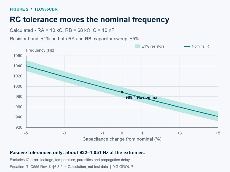
Imagine that the equipment accepts pulses from 900Hz to 1,100Hz. The passive-only calculation leaves some margin, which the remaining error terms and tests must address. If the equipment instead needs 980Hz to 1,000Hz, the same passive selections already deserve attention before purchasing starts an alternate search. A tighter acceptance window does not become achievable merely because a second timer has the same nominal threshold ratios.
Those acceptance windows are hypothetical. In a real project, derive the limits from the function receiving the pulse: a display update, a test sequence, a timeout or another defined task. Preserve high and low interval limits if the receiving circuit cares about them separately. A frequency measurement alone can hide a duty-cycle problem.
It is often more productive to improve the timing capacitor specification, define the load and record the allowable interval than to collect a long list of nominally similar timers. That work can reveal margin problems in the current circuit before a substitution is even proposed. It also makes later comparison tests meaningful because the team knows which difference would actually cause a problem.
A useful alternate list creates options the team can evaluate. It does not promise that every listed part is interchangeable. The four candidates below are distinct timer families with publicly identifiable ordering codes. None has been qualified here as a replacement on an actual TLC555CDR board.
Table 4. Four comparison candidates for a TLC555CDR design.
| Exact candidate | Manufacturer | Verified reason to compare | First engineering question | Source |
|---|---|---|---|---|
| NE555DR | Texas Instruments | Standard single timer in eight-pin SOIC, commercial temperature | Does the design accommodate its specified supply and loaded output behavior? | TI exact page |
| LMC555CMX/NOPB | Texas Instruments | Low-power CMOS timer in eight-pin SOIC, −40°C to 85°C | Are reset, output levels and RC behavior acceptable over the required conditions? | TI exact page |
| TLC551CD | Texas Instruments | Related low-voltage CMOS timer in eight-pin SOIC, tube carrier | Can the electrical design and assembly process accept this different option? | TI exact page |
| TS555IDTTR | STMicroelectronics | Single CMOS timer, listed in SO-8 with industrial grade | What changes in footprint, electrical limits and production qualification across suppliers? | ST product page |
Sources checked September 23, 2026. Product-page characteristics establish comparison value; they do not establish complete pin, footprint, timing or system compatibility.
The NE555DR comparison is useful where engineers are tempted to treat “555” as a complete specification. Its TI page describes operation from 5V to 15V. That already raises a concrete question for a board using the TLC555C at a lower voltage. Familiar function and familiar package do not resolve the supply difference. The actual load and power budget need their own review.
LMC555CMX/NOPB is a more natural place to investigate a low-power CMOS alternative. Its ordering page identifies the SOIC version and a wider temperature range. The procurement value comes from a real, specific candidate the engineer can evaluate, rather than an unspecified family reference. A wider listed range still does not prove matching behavior at the boundaries of the original circuit.
TLC551CD introduces a different practical concern: the identified ordering option is tube supplied. That may suit a prototype bench and complicate an automated production line. TI's page also contains recommendation-card wording about pinout that is not enough to certify compatibility. Keep it as a candidate until the exact package and electrical documentation are reconciled. A sales-page comparison label should never become the sole engineering release record.
TS555IDTTR adds a second manufacturer's CMOS timer to the discussion. ST's public page identifies the exact ordering option and SO-8 industrial grade. It creates a credible cross-vendor investigation, provided the team checks the package drawing, pin assignments, electrical conditions and assembled-board behavior. Supplier diversity is useful when the resulting circuit has actually been evaluated.
In practice, choose the candidate that best matches the difficult requirement first. For a low-voltage product, supply behavior may dominate. For a fixture running from a stable rail, output loading and pulse acceptance may matter more. For a long-running assembly program, carrier format and release documentation can be the immediate obstacle. The best investigation order follows the product's constraint, rather than a uniform ranking of timer brands.
If the approved TLC555CDR continues to meet the product's needs and the supplier can provide a suitable dated offer, the immediate work is ordinary replenishment. Confirm the code, carrier, required quantity, shipment plan and documentation. There is no engineering benefit in reopening a settled circuit solely because a new fab appears in the news.
A product change requires a different conversation. TI's published PCN process describes identifying affected products, the reason for change, anticipated impact, qualification information and projected production shipments. An applicable notice can therefore connect a manufacturing development to a specific device. The article has not established any TLC555CDR-to-SM1 transfer. Ask for the actual affected-product evidence if that relationship matters to your approval process. TI PCN information.
For an urgent order, state the use case before comparing quotes. A maintenance team needing a few devices can have different carrier needs from a contract manufacturer feeding a production run. The difference is logistical, but it can determine whether the offered material is usable on the intended date. Keep quantity, handling and traceability requirements visible alongside the exact part number.
Table 5. Choose the next action from the actual obstacle.
| Current situation | Next action | Evidence needed before release | Avoidable mistake |
|---|---|---|---|
| Approved CDR offered in the required format | Confirm the dated commercial terms | Complete code, quantity, carrier and delivery record | Treating general availability as a reserved shipment |
| Legacy BOM names the CD tube option | Review the ordering and assembly change | Current option status, feeder implications and internal release | Declaring the entire family unavailable |
| Proposed different temperature grade | Review the complete operating-condition set | Supply, environment, electrical table and approval | Assuming a wider temperature label preserves every limit |
| Different timer proposed | Run an application-specific comparison | Pin/package review and timing, reset, load tests | Approving from a functional description alone |
| Manufacturing change claimed | Request the applicable product evidence | Affected ordering codes and change details | Assigning a fab from the press release alone |
Source: TLC555 Rev. K, TI's exact-device and PCN information; procurement actions are YG GROUP's editorial recommendations.
An evaluation batch should answer the open engineering question. Before ordering it, write down the board revision, supply conditions, connected load and allowed timing window. For an alternate, verify pin assignment and footprint first, then define the power-up, steady-state and reset tests that matter. That sequence prevents a promising room-temperature waveform from becoming an unsupported production approval.
Keep the original device as a reference under the same setup when available. Use the same timing components and measurement points for a direct circuit comparison; document any intentional component changes separately. If the alternate requires a different capacitor, the engineering decision concerns the modified circuit as a whole. Record that fact rather than presenting the result as a chip-only comparison.
A basic test record can be concise: identify the board and samples, state the conditions, capture frequency and high/low intervals, and record the outcome against the specified limits. Add temperature, supply ramp or interference checks where the product requirement calls for them. The point is to produce evidence the next engineer can interpret, not a large report with an unexplained “pass.”
The same discipline helps purchasing avoid a false choice between unlimited safety stock and an immediate redesign. A documented alternate evaluation, a clear next-build requirement and a confirmed shipment can each solve a different part of the problem. Their usefulness depends on the actual schedule and application. No assumed lead time or inventory target is needed to recognize those options.
Save the approved ordering code and carrier with the BOM revision, not just in an email thread. Attach the relevant change decision and note which alternatives were evaluated, under what conditions, and with which circuit changes. A candidate that passed one board revision may need review after a power-rail or load change.
When the next factory announcement arrives, the team can then compare it with an established baseline. That turns broad industry news into a focused question for the manufacturer or supplier. It also keeps routine replenishment from inheriting assumptions made during an earlier urgent buy.
Analog capacity news becomes useful when it helps the team decide what to buy, retain or evaluate. For TLC555CDR, that begins with an orderable device whose package, commercial-temperature range and carrier are understood. The current CDR/CD status distinction shows why the full code matters even inside a familiar timer family.
The engineering work is equally specific. Know the required supply and output load, define the allowed timing window, and separate passive tolerance from device and board effects. The RC example shows how a modest capacitor tolerance can consume meaningful timing margin before an alternate timer is considered. That observation is useful whether supply is comfortable or tight.
Use an alternate only after the actual circuit and assembly requirements support it. A smaller supplier list with clear evidence is more useful than several unqualified “equivalents.” Keep the existing design when it remains appropriate, investigate the most relevant fallback, and tie the next purchase to a dated commitment for the exact item.
For the next build, keep three things together: the approved BOM, its timing acceptance limits and the dated offer for the exact part.