
Jolin Zeng




| Picture | Part Number | Manufacturer | Stock | Action |
|---|---|---|---|---|
 | NVMFD5C674NLWFT1G | onsemi | 8,180 | |
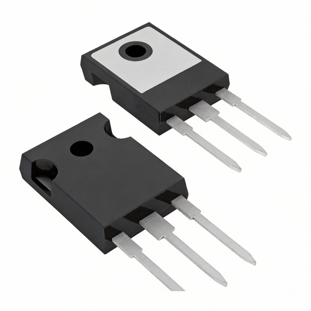 | NVMFD5C674NLT1G | onsemi | 1,650 |
No. The datasheet separately identifies NVMFD5C674NLWFT1G as the wettable-flank option. Preserve the full order code and check the matching device marking in Table 1.
No. An optical inspection feature supports a particular view of the soldered assembly. It does not establish the circuit's switching function, leakage, gate drive, or thermal operating margin. Define complementary inspection and electrical checks for the actual board.
No. The cited forecast concerns global equipment sales. It provides no order-code-specific stock, lead-time, allocation, or pricing information for NVMFD5C674NLT1G. Obtain those details from a dated, traceable offer and verify the offered package option.
NVMFD5C674NLT1G is an onsemi dual N-channel MOSFET supplied in a DFN8 package. Its close relative NVMFD5C674NLWFT1G adds the wettable-flank option identified for enhanced optical inspection. For an assembly or sourcing decision, preserve that suffix distinction and match it to the approved soldering, inspection, and electrical test process. Broad growth in semiconductor packaging investment does not establish that these two order codes can be exchanged without review. onsemi datasheet, pages 1 and 5.
SEMI's July 14, 2026 forecast projects worldwide semiconductor test-equipment sales of $15.3 billion in 2026, up 31.0%, and assembly-and-packaging equipment sales of $6.7 billion, up 9.6%. These are separate equipment-sales forecasts, not actual full-year results, packaged-chip revenues, or board-assembly output. SEMI mid-year equipment forecast.
For a buyer or manufacturing engineer, the practical lesson is to keep market context and component approval in different records. Industry investment can prompt questions about a supplier's capabilities, capacity, or process changes. The answers still need evidence for the particular package, manufacturing route, and order code being purchased.
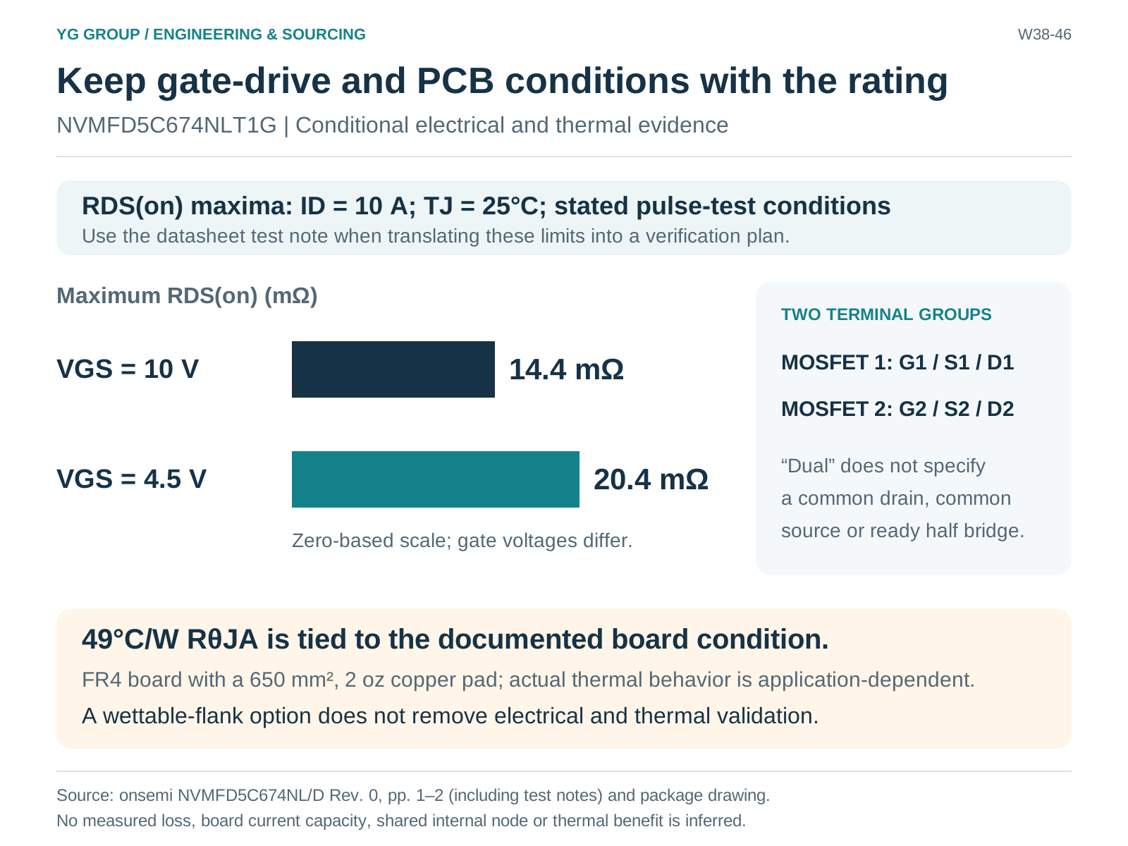
**Figure 1. The package suffix changes the inspection review.** YG Group comparison from onsemi NVMFD5C674NL/D Rev. 0. The WF option supports enhanced optical inspection; no detection rate, complete hidden-joint coverage, thermal improvement, lot conformity or substitution approval is claimed. Listed shipment formats describe the datasheet, not a current offer. Sources: [supporting source 1](https://www.onsemi.com/download/data-sheet/pdf/nvmfd5c674nl-d.pdf). **Figure 2. Keep gate-drive and PCB conditions with the rating.** Conditional maxima from onsemi NVMFD5C674NL/D Rev. 0, compiled by YG Group: ID 10 A, TJ 25°C and the datasheet pulse-test condition apply. The 49°C/W junction-to-ambient value uses the stated FR4 board with 650 mm², 2 oz copper pad. The figure does not assert actual board current capacity, an internal common-node topology or a thermal advantage for the WF option. Sources: [supporting source 1](https://www.onsemi.com/download/data-sheet/pdf/nvmfd5c674nl-d.pdf).NVMFD5C674NLT1G is a conventional power-device package example within that wider assembly-and-test discussion. The datasheet identifies a DFN8 5 × 6 mm class, SO8FL dual package. It provides no basis to describe this component as a chiplet, HBM, or advanced heterogeneous-integration product. onsemi datasheet, page 1 and Case 506BT.
This distinction is useful when a broad packaging story reaches a purchasing desk. It prevents an industry forecast from becoming an unsupported claim about this part's lead time, shortage risk, price direction, or manufacturing technology.
The datasheet's ordering table distinguishes the ordinary DFN8 version from the wettable-flank version. It also assigns different device markings. Both are listed with the same nominal shipment quantity and tape-and-reel format, but those common fields do not erase the package-feature difference.
| Ordering code | Datasheet package description | Device marking | Listed shipment format |
|---|---|---|---|
| NVMFD5C674NLT1G | DFN8, Pb-free | 5C674L | 1,500 / tape and reel |
| NVMFD5C674NLWFT1G | DFN8, Pb-free, wettable flanks | 674LWF | 1,500 / tape and reel |
Table 1: Exact ordering distinctions. Source: onsemi Device Ordering Information, page 5. Compiled by YG Group. Shipment format is the datasheet listing, not a statement about a particular offered lot.
Use the complete order code on the bill of materials, approved-parts list, purchase order, incoming-inspection instruction, and manufacturing record. An internal database that truncates both entries to NVMFD5C674NL can hide the very distinction that the inspection process depends on.
The component's short top marking is a cross-check, not a substitute for the full manufacturer label and traceability documents. The datasheet separately describes assembly-location, year, work-week, and lot-traceability fields. Match those records consistently; a familiar-looking short code alone does not establish lot authenticity or supplier authorization. onsemi datasheet, marking diagram and ordering table.
onsemi identifies the WF option as supporting enhanced optical inspection. That is a reason to evaluate NVMFD5C674NLWFT1G when the assembly process needs that package feature. It is not a statement that the primary NVMFD5C674NLT1G has wettable flanks, and it is not a quantified detection-rate guarantee. onsemi datasheet, Features.
A useful process review begins with the defect or joint characteristic that must be assessed. Determine which external joint features the optical system can inspect, which under-package connections need other evidence, and what the electrical test can establish. Do not infer the condition of every hidden solder connection from an acceptable visible edge.
For a proposed wettable-flank change, manufacturing should verify the actual package revision, land pattern, paste process, inspection recipe, and acceptance criteria. Trial assemblies should demonstrate that the chosen process produces inspectable joints and that the inspection system distinguishes the targeted conditions. These are proposed engineering checks; no inspection yield, defect-escape rate, or production trial is reported here.
The economic comparison should include that process work. A small component-price difference can be less important than requalification effort or a poorly defined inspection requirement, but neither cost nor savings can be calculated without the factory's own data. The useful purchasing question is therefore: Which exact package option has an approved, demonstrable inspection process for this board?
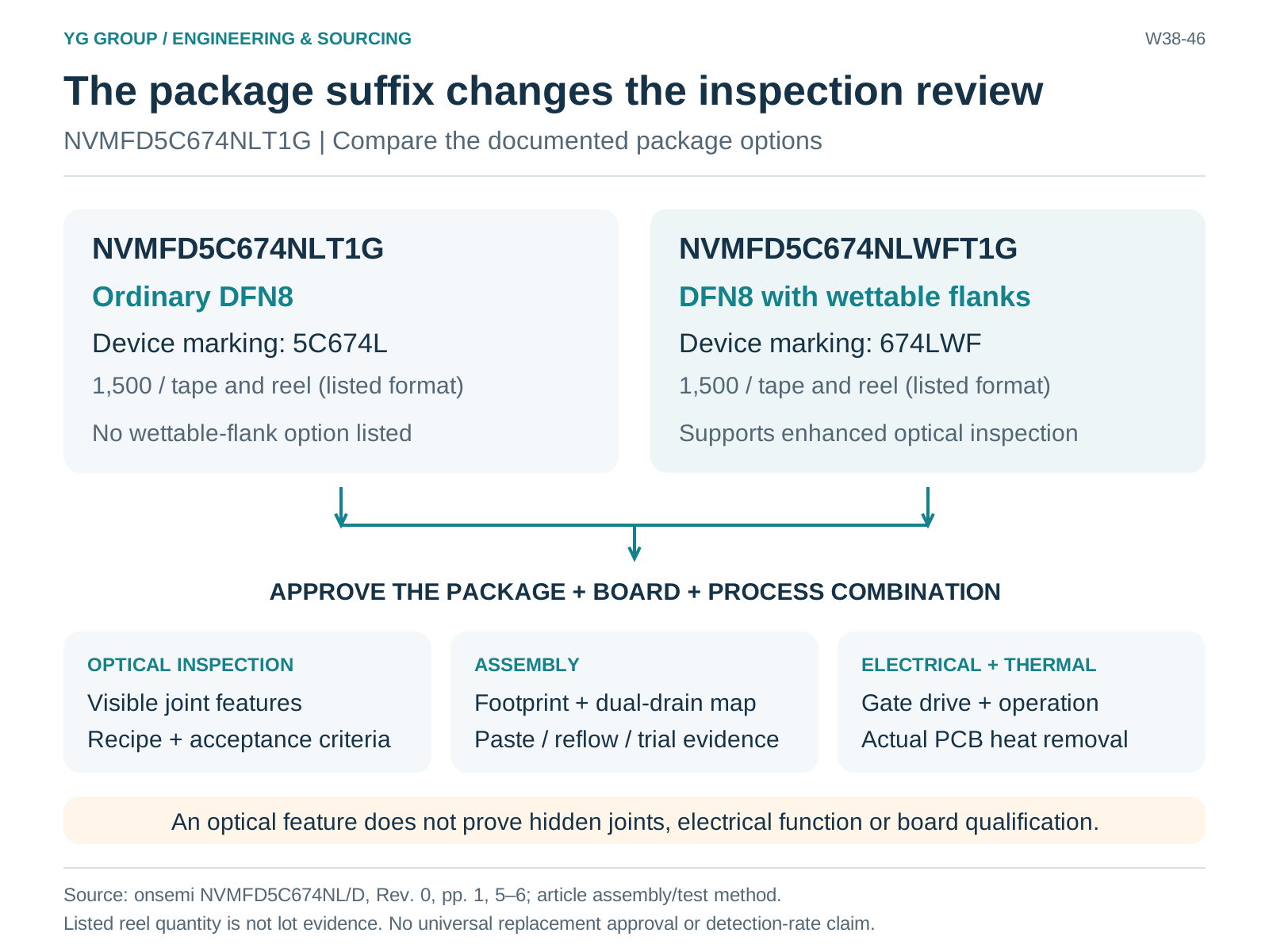
The package contains two N-channel MOSFETs. The datasheet symbol presents separate G1/S1/D1 and G2/S2/D2 terminals, and the package drawing identifies the dual-flag structure. Verify the schematic and footprint against those connections, including the two drain regions. Do not infer a common drain, common source, or ready-made half bridge from the word “dual.” onsemi datasheet, page 1 and package drawing.
Package selection also cannot be isolated from thermal and electrical requirements. The electrical table gives maximum RDS(on) of 14.4 mΩ at VGS = 10 V and 20.4 mΩ at VGS = 4.5 V, both at ID = 10 A and TJ = 25°C under the stated pulse-test condition. Preserve the gate-voltage and temperature conditions when checking conduction loss or a production-test limit. onsemi datasheet, Electrical Characteristics and note 4.
Likewise, the 42 A headline is associated with a case-temperature condition. The ratings table separately lists 11 A with ambient at 25°C under its board-related conditions. These are not two interchangeable current promises for an arbitrary PCB, and adding the two transistor headlines does not establish an 84 A board rating. Evaluate each device's dissipation and the package/board thermal behavior in the actual circuit. onsemi datasheet, Maximum Ratings, notes 1–3.
The specified 49°C/W junction-to-ambient thermal resistance refers to an FR4 board with a 650 mm², 2 oz copper pad. The datasheet expressly makes thermal values dependent on the application environment. An optical-inspection-friendly package option does not remove the need to validate copper area, solder attachment, neighboring heat sources, and operating temperature.
The datasheet states AEC-Q101 qualification and PPAP capability. Those manufacturer statements do not establish that a particular finished board has passed its required qualification or that a customer-specific PPAP submission has been supplied and approved. Keep the supplier's component evidence, the assembly-process evidence, and the final product's acceptance evidence distinct. onsemi datasheet, page 1.
For the same reason, do not turn a maximum soldering-related rating into a complete reflow recipe. The datasheet's lead-temperature entry includes a location and duration condition; it does not define the whole assembly profile. Use applicable manufacturer assembly guidance and the qualified factory process when setting the profile, rather than copying a single temperature from the maximum-ratings table.
The following record provides a practical way to connect purchasing and manufacturing decisions without mixing those evidence types.
| Approval question | Evidence to retain | What remains unproven without it |
|---|---|---|
| Which package was ordered? | Full OPN, manufacturer label, approved supplier and lot records | Whether the received option matches the approved BOM |
| Does the footprint match? | Applicable case drawing, pad mapping, PCB revision | Correct dual-drain connection and mechanical fit |
| Can the joints be assessed as required? | Agreed acceptance criteria, inspection recipe, trial records | Detection coverage for the selected package and process |
| Is the assembly process suitable? | Qualified paste/reflow process and relevant assembly guidance | Soldering robustness on the actual board |
| Does the circuit operate within limits? | Electrical and thermal validation at required conditions | Functional performance beyond a visually acceptable joint |
| Is a suffix change approved? | Engineering-change decision and affected-record updates | Permission to substitute the wettable-flank and ordinary options |
Table 2: Proposed approval record, compiled by YG Group from the datasheet's ordering, pin, electrical, thermal, and mechanical information. This is an engineering workflow, not an onsemi-mandated inspection standard or a completed YG Group test.
Consider a purchase request for NVMFD5C674NLT1G that receives an offer for NVMFD5C674NLWFT1G. The correct first response is to identify the wettable-flank difference and check the existing approval scope. Shared family electrical information is useful, but it does not itself approve the board's footprint, inspection program, labeling, or customer documentation for the alternative.
The reverse direction can be more revealing. If a process was approved around a wettable-flank option, accepting the ordinary T1G part merely because the headline voltage and resistance match can remove an expected inspection feature. That is a process question even when no change to the nominal circuit function is intended.
Document the reason for the choice and any revalidation required. A defensible decision can retain either option when the evidence supports the required process. The article does not declare one universally better, cheaper, or immediately available.
For NVMFD5C674NLT1G, an effective assembly-and-test decision starts with the complete suffix and ends with a documented process that can inspect and validate the intended board. Use the wettable-flank relative as a specific package comparison, retain the conditions behind the electrical and thermal ratings, and keep market forecasts separate from lot-level purchasing evidence.
Author: Jolin Zeng