
Doris Lee




| Picture | Part Number | Manufacturer | Stock | Action |
|---|---|---|---|---|
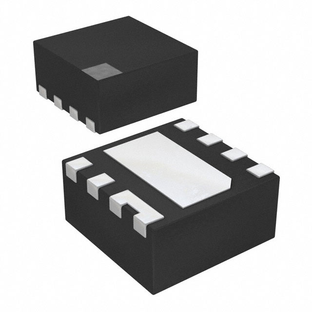 | NCP45524IMNTWG-H | onsemi | 9,520 | |
 | NCP45524IMNTWG-L | onsemi | 3,640 |
No. It is a controlled load switch. Its specified input range and integrated power path support evaluating a suitable local domain; they do not provide voltage regulation or establish suitability for a GPU core power stage.
The documented PG condition is that the MOSFET gate is fully charged. A downstream voltage-tolerance or reset requirement needs the relevant voltage-monitoring evidence and system validation.
No. The IEA source describes data-centre electricity use. It supplies no NCP45524IMNTWG-H stock, allocation, price, or lead-time information. A sourcing decision needs a dated offer with the exact order code and traceability evidence.
NCP45524IMNTWG-H is an onsemi load switch with active-high enable and an open-drain power-good output. It can support sequencing of suitable low-voltage power domains on a server board, provided the design checks what that output actually indicates, the startup current, and the thermal conditions. Its role is local power switching: the datasheet's server application does not establish use in a particular AI platform or make it a GPU core regulator. onsemi datasheet, pages 1–3 and 14.
The IEA's April 16, 2026 Key Questions on Energy and AI reports that global data-centre electricity demand grew 17% in 2025, while electricity use by AI-focused data centres grew 50%. Its central projection puts total data-centre consumption at about 950 TWh in 2030, versus 485 TWh in 2025. These are electricity-demand estimates and projections, not server-unit shipments or demand forecasts for this load switch. IEA executive summary.
That industry context makes power management a useful engineering subject. It does not identify which components a server maker has selected. The relevant question for NCP45524IMNTWG-H is narrower:
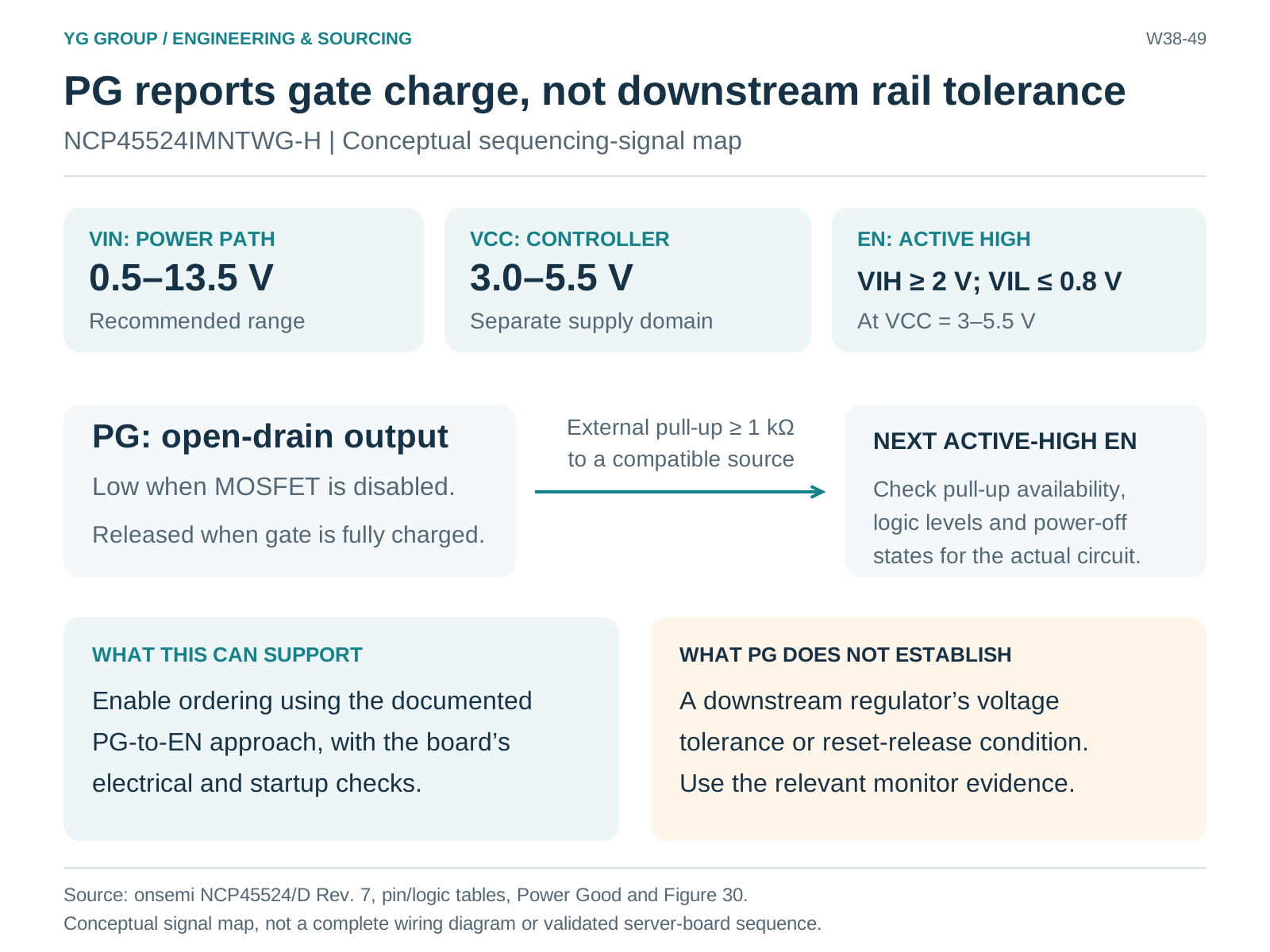
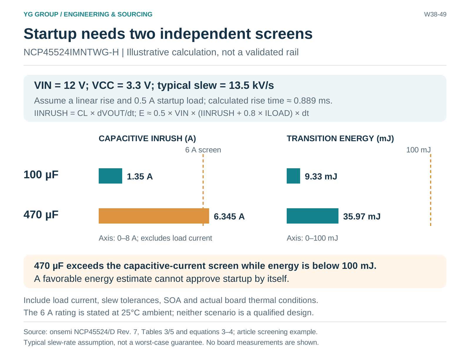
**Figure 1. PG reports gate charge, not downstream rail tolerance.** YG Group synthesis of onsemi NCP45524/D Rev. 7. PG is low when the MOSFET is disabled and released when its gate is fully charged; it requires an external pull-up of at least 1 kΩ to a compatible source. This conceptual map does not replace the complete manufacturer circuit, startup sequencing, receiver-level and power-off review, nor does PG establish a downstream regulator’s voltage tolerance. Sources: [supporting source 1](https://www.onsemi.com/download/data-sheet/pdf/ncp45524-d.pdf). **Figure 2. Startup needs two independent screens.** Illustrative calculations from the article using onsemi Rev. 7: VIN 12 V, VCC 3.3 V, typical slew 13.5 kV/s, a linear 0–12 V rise and 0.5 A startup load. The plotted current is capacitive inrush only; total switch current includes load current. The 6 A rating is stated at 25°C ambient. Actual waveforms, tolerances, SOA and board thermals remain required; neither row constitutes operating approval. Sources: [supporting source 1](https://www.onsemi.com/download/data-sheet/pdf/ncp45524-d.pdf).The answer requires a rail definition, not an AI label. Record the domain's input voltage, controller supply, load current before and after startup, effective capacitance, downstream reset requirements, and permitted power-off behavior. A storage, management, or peripheral domain is a possible design context to evaluate, not a documented design win for this device.
NCP45524 integrates an N-channel MOSFET with its control and drive circuitry. The recommended operating range is 0.5–13.5 V for VIN and 3.0–5.5 V for VCC. VIN is the power path; VCC powers the controller. A 12 V switched rail therefore does not justify connecting 12 V to VCC. The 18 V absolute-maximum VIN entry is likewise not an 18 V operating recommendation. onsemi datasheet, pin description and Tables 2–3.
The package is DFN8, 2 × 2 mm, Case 506CC. Pin 1 and the exposed VIN pad, pin 9, must be connected. Pins 7 and 8 are VOUT. Verify the pad connection and copper implementation against the pin description and mechanical drawing, rather than treating the exposed pad as an unspecified ground or purely mechanical feature. onsemi datasheet, pages 2 and 16.
The 6 A continuous-current entry is stated at ambient 25°C. It does not guarantee 6 A on every compact server-board footprint or at every local temperature. Check startup current, steady-state dissipation, the safe operating area, and board heat removal as separate conditions.
For NCP45524IMNTWG-H, driving EN high enables the MOSFET when VCC is adequate; driving it low disables the MOSFET. An internal pull-down biases an undriven EN toward the disabled state. The specified logic thresholds are VIH = 2 V minimum and VIL = 0.8 V maximum over VCC = 3–5.5 V. Check the driving controller's guaranteed levels, including its own startup state. onsemi datasheet, Tables 1 and 4, Enable Control.
The PG output is more specific than its name may suggest. It indicates that the MOSFET gate is fully charged. It is an active-high, open-drain output that requires an external pull-up of at least 1 kΩ to a compatible voltage source. It is pulled low when the MOSFET is disabled and released when the gate is fully charged. This is not a specified voltage-window monitor for a downstream regulator's output. onsemi datasheet, pages 2–3 and Power Good.
Figure 30 shows PG from one NCP45524-H driving the enable of another active-high device. This provides a useful sequencing mechanism, but the board still needs a definition of “ready.” If the requirement is that a downstream regulated rail has reached a particular tolerance before reset is released, use evidence from the appropriate regulator or supervisor. Do not replace that condition with a gate-charge indication merely because the signal is named PG.
For a PG-to-EN connection, review the pull-up supply's availability, receiver thresholds, sink current, input loading, and power-off states. The datasheet's minimum pull-up resistance is one boundary; it does not make every larger resistance suitable for every node capacitance and required edge time. If PG is unused, the datasheet instructs that it be tied to GND. onsemi datasheet, page 10 and Figure 30.
The application section recommends VCC before EN for specified performance, with VIN supplied either before VCC or after EN. It also states that VCC must have reached at least 2 V when EN is asserted so that enable latches correctly; asserting EN too early may not take effect. This latch condition does not lower the recommended VCC operating minimum of 3 V. The same section recommends a minimum 10 ms interval between the power-sequence steps for internal stabilization. onsemi datasheet, Power Sequencing.
These instructions address the device's initial power application. They should not be confused with the typical PG timing after an enable transition. For example, the switching table lists a typical 1.33 ms PG turn-on time at VCC = 3.3 V and VIN = 12 V, with VTERM = VCC, RPG = 100 kΩ, RL = 10 Ω, and CL = 0.1 µF at TJ = 25°C. The timing diagram defines the measurement from EN to PG. This is neither a guaranteed maximum for a loaded server board nor a replacement for the initial supply-sequencing recommendation. onsemi datasheet, Table 5 and Figure 2.
Capture VCC, EN, VIN, VOUT, and PG together during board validation. Include a cold start, a restart while downstream capacitors retain charge, and the actual power-off sequence. These are proposed verification cases; no board measurements are claimed here.
Controlled output slew rate limits the capacitive charging component of inrush. That description does not establish a separately regulated, programmable current-limit threshold. The datasheet requires the capacitive inrush to remain below the specified current limit and separately constrains OFF-to-ON transition energy. onsemi datasheet, Capacitive Load and transition-energy discussion.
A first screening calculation uses the datasheet relations:
IINRUSH = CL × dVOUT/dt
E ≈ 0.5 × VIN × (IINRUSH + 0.8 × ILOAD) × dt
Here dt is the output's full rise time from 0 V to VIN; ILOAD is the load current used in the manufacturer's transition approximation. The recommended operating table limits transition energy to 100 mJ. That energy limit does not override the current rating or the safe operating area. onsemi datasheet, Table 3 and equations 3–4.
Consider an illustrative 12 V domain with VCC = 3.3 V. Use the listed typical slew rate of 13.5 kV/s, assume a linear rise, and assume 0.5 A load current during startup. Those assumptions give dt ≈ 0.889 ms. The following are calculated screening values, not measurements or validated operating points.
| Effective load capacitance assumed | Calculated capacitive inrush | Approximate transition energy | Initial interpretation |
|---|---|---|---|
| 100 µF | 1.35 A | 9.33 mJ | Below these two headline limits; full validation remains necessary |
| 470 µF | 6.345 A | 35.97 mJ | Fails the 6 A capacitive-current screen despite being below 100 mJ |
Table 1: Illustrative startup screening, calculated by YG Group using Table 5 and equations 3–4. Assumptions: VIN = 12 V, VCC = 3.3 V, typical slew rate 13.5 kV/s, linear 0–12 V rise, ILOAD = 0.5 A. No allowance for tolerances or a nonlinear startup load is included.
The second row shows why one favorable number cannot approve startup. Total switch current also includes load current, and the actual ramp, capacitance, temperature, and rail behavior must be evaluated. Because the quoted slew rate is typical rather than a guaranteed corner bound, even the first row is a preliminary screen. Check the actual waveform against the safe-operating-area information and evaluate repeated starts rather than treating a single-transition energy calculation as a repetitive rating.
The BLEED connection discharges the load when the MOSFET is disabled. The datasheet requires BLEED to connect to VOUT directly or through an external resistor no greater than 100 MΩ. The external resistor can slow discharge and reduce dissipation in the internal bleed resistor. onsemi specifies a 0.4 W maximum continuous dissipation for that internal resistor. onsemi datasheet, Load Bleed.
Define how low VOUT must fall before the next start, and how long the system can wait. Check for energy fed into the domain through another supply or interface; do not assume a quick-discharge feature guarantees the domain is unpowered. An externally sustained output is a different condition from discharging an isolated capacitor.
For conduction loss, the datasheet gives RON = 21.9 mΩ typical and 31.7 mΩ maximum at VCC = 3.3 V, VIN = 12 V, and TJ = 25°C. Retain those conditions when starting an I²R estimate, then account for temperature and PCB resistance. The two listed junction-to-ambient values, 40.0°C/W and 72.7°C/W, refer to different copper-pad conditions; neither is a universal property of the package alone. onsemi datasheet, Tables 2 and 4 and layout guidance.
The local server-board environment matters more than a facility-level energy statistic at this stage. A hot location near another power stage can invalidate a room-temperature current assumption even though the aggregate data-centre market is growing.
| Exact order code | Pin 6 | Enable polarity | Sequencing consequence |
|---|---|---|---|
| NCP45524IMNTWG-H | PG | Active high | Primary device; supports the documented PG-to-active-high-enable approach |
| NCP45524IMNTWG-L | PG | Active low | Control polarity changes; not a direct swap in the same enable logic |
| NCP45525IMNTWG-H | SR | Active high | Pin 6 adjusts slew rate instead of providing PG; the sequencing circuit must change |
Table 2: Same-family differences, compiled by YG Group from onsemi Ordering Information, page 14. The table compares documented functions and does not approve substitution.
NCP45525 is worth evaluating when a slower adjustable ramp is required, but its SR function cannot serve as the primary device's PG signal. Revision 7 also distinguishes NCP45525 slew-rate-control constants for material before and after the change identified as FPCN26053XD. A design using that alternative needs the applicable material/change information and the appropriate constant; this article does not assign a change status to any offered lot. onsemi datasheet, Table 4 notes 14–15 and revision history.
NCP45524IMNTWG-H offers a concrete way to investigate local server-board power sequencing. Start with separate VIN and VCC requirements, define PG according to its gate-charge function, and verify startup current, transition energy, shutdown behavior, and board temperature. Preserve the full order code when discussing alternatives. That approach turns a broad AI-demand topic into a testable power-domain decision without claiming a design win or a component shortage.
Author: Doris Lee