
Evan Huang




| Picture | Part Number | Manufacturer | Stock | Action |
|---|---|---|---|---|
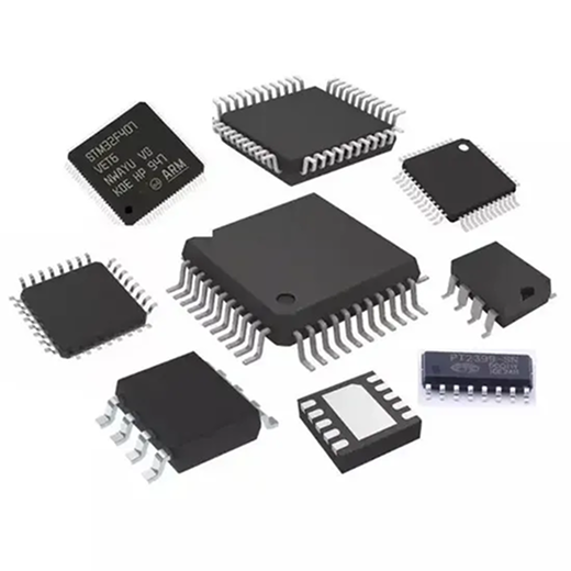 | MT29F64G08AFAAAWP-ITZ:A | Micron | 6,720 | |
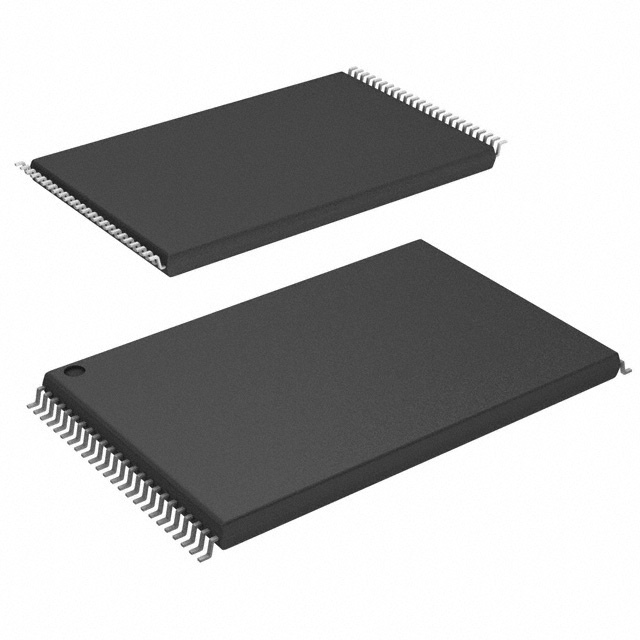 | MT29F32G08ABAAAWP-ITZ:A | Micron | 5,180 | |
| MT29F128G08AJAAAWP-ITZ:A | Micron | 9,500 | |
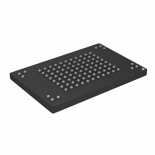 | MT29F64G08AECABH1-10ITZ:A | Micron | 1,940 | |
| MT29F32G08ABCABH1-10ITZ:A | Micron | 6,010 |
No. A company announcement or an industry forecast can describe broad demand and investment without reporting availability for MT29F64G08AFAAAWP-ITZ:A. Its sourcing position needs dated evidence for the complete ordering code, quantity and delivery conditions. For an existing design, review technical alternatives early, but distinguish an already qualified option from one that still needs firmware changes or a new PCB. Neither a family datasheet nor an indexed catalog row establishes a current delivery commitment.
No. The device has a 64Gb main array, equivalent to 8GiB before bad blocks and host reserves. Its WP suffix identifies the 48-pin TSOP configuration, which supports the asynchronous interface only. Synchronous transfer specifications elsewhere in the M73A family document apply to different configurations. The primary device uses two targets, one LUN per target and a shared x8 data bus; the host must support both chip enables to access the complete device.
The applicable M73A datasheet specifies at least 8-bit ECC per 540 bytes of data. Check that wording against the controller's protected codeword, correction strength, parity storage and boot format. Each page has 8192 main bytes plus 448 spare bytes, but the spare area is not simply free application space. Factory markers, parity and management metadata must coexist without conflicting with the bootloader or manufacturing programmer. An ECC engine's headline correction number alone does not establish compatibility.
By Evan Huang
MT29F64G08AFAAAWP-ITZ:A is a Micron 64Gb SLC NAND device for hosts that manage raw flash themselves. Its relevance to a supply discussion comes from the work already invested in that host: two chip enables, an asynchronous interface, an 8KB page and a specific ECC requirement. Broad NAND market signals can prompt an earlier purchasing review, but a useful sourcing decision starts with those engineering commitments and the cost of changing them.
A purchasing team can read a strong memory market forecast and still have very little information about its own bill of materials. The practical question is whether the forecast changes an order, a qualification schedule or the amount of engineering effort worth spending on another device. For a mature parallel NAND design, the answer usually depends on information much closer to the product than an industry revenue chart.
Micron's June 24, 2026 fiscal third-quarter announcement describes growing customer demand and increased investment in technology, products and supply. Its product highlights include G9 NAND-based SSD developments. Those are meaningful signals about the company's priorities, but the announcement does not give a shipment forecast, allocation level or delivery commitment for this particular 48-pin SLC device. Micron's fiscal Q3 2026 announcement supplies the industry context used here.
*Figure 1. Conceptual host responsibilities for the primary dual-target TSOP configuration. The shared x8 bus is separate from target selection; ECC and bad-block management remain host responsibilities. Based on Micron M73A Rev. L, pages 26, 32 and 110, [Micron M73A datasheet](../规格书/W38-38.pdf). Diagram: YG GROUP; not a package pinout.* *Figure 2. Proposed qualification sequence for a raw NAND sourcing decision. Each gate creates evidence needed by the next; a failed gate returns the candidate for correction or exclusion. Based on the host requirements in [Micron's M73A documentation](../规格书/W38-38.pdf), with workflow designed by YG GROUP. No qualification duration or completed hardware test is claimed.*The family table gives the same listed READ ID sequence for the asynchronous 32Gb single-die and 64Gb dual-die configurations. It therefore cannot, by itself, identify the entire package topology. The host needs the correct board configuration and parameter-page information from each connected target, with CRC validation. Qualification should exercise both targets and their address boundaries. A successful read from the beginning of flash does not demonstrate that all storage is present or correctly mapped.
Yes. Read and preserve the factory markers before programming or erasing. For this family, the first spare location at byte 8192 in the first page carries the specified bad-block marker. Erasing first can destroy information the host needs. The datasheet allows factory-invalid blocks and specifies a minimum valid-block count, so acceptance must distinguish permitted factory marking from new failures. Usable capacity must also allow for software metadata, recovery copies and the product's chosen reserves.
Compare MT29F32G08ABAAAWP-ITZ:A for lower-density asynchronous TSOP use and MT29F128G08AJAAAWP-ITZ:A for higher density with different LUN organization. MT29F64G08AECABH1-10ITZ:A and MT29F32G08ABCABH1-10ITZ:A are related BGA options with 1.8V I/O. The first pair still requires capacity, addressing and boot review; the BGA pair also requires hardware redesign. These are engineering comparison candidates, not approved drop-in replacements. Check the complete part identity and application requirements before adding any candidate to an approved list.
The distinction matters because NAND capacity is not a universal pool that every product can draw from without qualification. A finished SSD, a raw parallel SLC package and a host-managed storage subsystem solve different problems. A design using this part cannot consume an SSD supply increase simply by substituting a purchase-order line. The processor interface, boot sequence, board layout and software ownership would change.
Our view is that qualification flexibility is the most useful response to uncertain supply. A team that knows which substitutions are feasible can negotiate and plan with more options. A team that merely collects nominally similar part numbers may discover, during a shortage, that none of those options can boot its existing board.
Table 1. Separate the market signal from the decision it can support.
| Information available | What it helps establish | What the buyer still needs |
|---|---|---|
| Manufacturer financial announcement | Broad demand, investment and product priorities | Exact ordering-code supply evidence |
| Manufacturer family datasheet | Device behavior and engineering constraints | Applicability to the complete suffix and host |
| Catalog entry for an exact part | Identifiable product configuration | Dated lifecycle and delivery confirmation |
| Supplier quotation | An offer for specified quantity and conditions | Traceability, lot identity and acceptance terms |
| Completed board qualification | Compatibility with the tested hardware and software | Change control for later lots and revisions |
Source: Micron's announcement, SLC NAND catalog and YG GROUP's engineering interpretation. This is an evidence map, not a measured supply ranking.
A dated quotation and a released firmware build belong in the same discussion. If another device needs a new bootloader, that work has a schedule and a failure mode. If the existing device already satisfies the application, changing it solely because a different capacity appears cheaper can transfer expense from purchasing to firmware, test and field support. Compare the cost of storage the product can actually use, including the software and test work.
The primary part has a 64Gb main array, equivalent to 8GiB before bad-block allowance, management structures and application reserves. The lowercase “b” is consequential: this is not a 64GB device. Its x8 interface transfers one byte across eight data pins, and the WP package code denotes a 48-pin TSOP. The IT temperature option is industrial, from −40°C to +85°C.
The M73A family document covers several densities, package arrangements and interfaces. Reading its first-page maximum speed as a property of every ordering code would give the wrong answer here. This TSOP version supports the asynchronous interface only. The family also contains synchronous BGA devices, but their interface capability does not transfer to the primary model. The package notes and parameter-page tables explicitly distinguish them.
The F configuration uses two dies, two chip enables and two ready/busy signals with common data I/O. Each chip enable addresses one logical unit, or LUN. A LUN is the internal unit whose array operations and status the controller must manage. Both targets share the external byte-wide data bus, so the design needs correct selection and bus ownership as well as enough address space.
Table 2. Primary-device facts that change the host design.
| Property | Applicable configuration | Why it matters |
|---|---|---|
| Main-array density | 64Gb, equivalent to 8GiB raw main data | Storage exposed to the application will be smaller |
| Interface | Asynchronous x8; no synchronous TSOP operation | Match controller timing and boot-ROM support |
| Supply configuration | VCC and VCCQ nominally 3.3V; specified 2.7–3.6V | A 1.8V I/O alternative needs electrical changes |
| Internal arrangement | Two targets, one LUN per target, common I/O | Both chip enables must be supported and enumerated |
| Page geometry | 8192 main bytes plus 448 spare bytes | DMA, ECC and spare-area layout must agree |
| Block geometry | 128 pages, 4096 blocks per LUN | Erase management works at a large physical granularity |
| Temperature option | IT: −40°C to +85°C | Industrial scope does not establish automotive qualification |
Source: Micron M73A datasheet, Rev. L, April 2026, pages 2, 13, 26, 32 and 65–66; supplied Micron M73A document. The supplied project copy is the version used for this analysis.
The process suffix also belongs in the controlled identity. In this document, Z denotes a polyimide process option, while the colon suffix identifies a design revision. That does not by itself imply an incompatibility between every suffix combination. It means a buyer should preserve the complete approved code rather than silently shorten it and assume the remaining text defines the same orderable item.
A sensible receiving record therefore links the purchase description, manufacturer label, lot information and approved drawing or datasheet revision. This is useful even when the electrical design remains unchanged. If an issue later appears in programming yield, the team can distinguish a software change, an assembly change and a received-material difference instead of treating all flash devices as one undifferentiated batch.
A storage driver running under a full operating system may support many NAND geometries. The processor's immutable boot ROM often supports fewer. This difference can make an otherwise attractive substitute unusable before any operating-system driver has a chance to run. Establish what reads the first executable bytes, which chip enable it uses and how it interprets page data and error correction.
For an existing product, start with its actual boot image format and controller configuration. Determine whether the boot ROM reads a parameter page or expects fixed geometry. Check whether it uses a vendor-specific ID table, a fixed spare-area layout or an ECC engine with a limited correction strength. A driver entry that recognizes the manufacturer is not enough to show that the complete boot chain handles this device.
Micron's power-up sequence requires a RESET command to each target before normal operation. The device then provides ONFI parameter information that should be read with its CRC checked. Redundant parameter-page copies support recovery from a bad read. They do not justify accepting arbitrary data merely because the first four bytes look familiar. The host should reject inconsistent geometry and retain useful diagnostics for the failure.
There is a particularly practical trap in the family identification table: the 32Gb asynchronous single-die configuration and the 64Gb asynchronous dual-die configuration share a listed READ ID sequence. READ ID alone is not a complete description of package capacity or target topology. Board configuration and per-target parameter discovery must resolve the arrangement that is actually connected. The supplied Micron M73A document covers these identification and power-up requirements on pages 50–51 and 60–66.
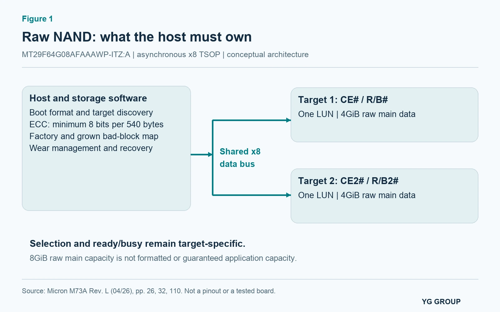
The diagram also explains why testing only the first few megabytes is weak evidence. A short test can exercise one target, one region and a narrow set of addresses while leaving the second target completely untested. A qualification image should write recognizable patterns across both targets and verify that addresses neither alias nor disappear at the target boundary.
Recovery deserves the same attention as a clean start. Interrupt power during image installation, restart with an incomplete update and confirm that the product reaches a defined recovery state. The exact implementation depends on the product, but its acceptance criterion should be clear: an interrupted operation must not make every boot copy inaccessible. Keeping multiple copies is useful only when the boot software knows how to find and validate them.
Raw NAND exposes responsibilities that a managed storage device would hide. Error correction, bad-block mapping and wear management have to work together. Each subsystem can appear correct in isolation while the complete format fails. A hardware ECC engine may generate parity successfully, for example, but place it where an older bootloader expects a factory bad-block marker.
The applicable datasheet specifies a minimum of 8-bit ECC per 540 bytes of data. That wording should survive the requirements review. Rewriting it casually as “8 bits per 512 bytes” discards the protected-data convention that the implementation must resolve. The controller's advertised correction strength, codeword coverage, parity size and spare-area handling need to be checked as a set.
The page contains 8192 main bytes and 448 spare bytes. Dividing those quantities into sixteen equal groups yields 512 main bytes and 28 spare bytes per group, or 540 bytes together. That arithmetic helps explain the geometry, but it is not a prescribed parity layout. The ECC algorithm, controller format and boot requirements determine how the spare bytes are assigned and which bytes receive protection.
Table 3. Geometry calculations and the decisions they support.
| Item | Calculation or requirement | Design consequence |
|---|---|---|
| Physical page payload plus spare | 8192 + 448 = 8640 bytes | Transfer buffers must distinguish main and spare data |
| Main data per erase block | 8192 × 128 = 1MiB | Small updates can cause much larger erase and relocation work |
| Main array per LUN | 4096 × 1MiB = 4GiB | Two targets together provide 8GiB raw main data |
| Equal page subdivision | Sixteen groups of 512 + 28 bytes | Useful layout arithmetic; not an automatic ECC format |
| Minimum valid blocks | 4016 of 4096 per LUN | Budget capacity below the ideal physical block count |
| Factory marker | First spare location, byte 8192 of the first page | Preserve and inspect it before programming or erasing |
Source: Micron M73A Rev. L, pages 32 and 110, Micron M73A datasheet. Arithmetic compiled by YG GROUP; usable capacity also depends on the host format and reserves.
The factory marker is especially easy to lose in a careless production process. A bulk erase performed before reading the original markers can destroy information the manufacturer intended the host to preserve. The datasheet directs software to examine the first spare location of the first page of each block before program or erase operations. Build the initial bad-block map first, then let the programming flow operate on eligible blocks.
A fresh part is allowed to contain factory-invalid blocks. Rejecting every unit with any bad block would misunderstand raw NAND; accepting a device without respecting the valid-block specification would be equally wrong. The manufacturing procedure should distinguish expected factory marking from a failed program, a new erase failure and a communication problem. Those events need different responses and different records.
Application capacity is another place where early clarity prevents an expensive argument. Two LUNs at the minimum valid-block count give 8032MiB of main-area blocks before software reserves. That is a planning floor derived from the geometry, not a formatted capacity promise. Boot copies, mapping metadata, future bad-block allowance and free space for garbage collection consume additional room. Publish the capacity the application can rely on, rather than the largest number visible on the component description.
The programming station must obey the same NAND rules as the product, even if it reaches the device through a different adapter. Confirm that its device profile includes both targets, the correct page and spare geometry, and the ECC representation expected by the released firmware. A station can verify its own output successfully while producing a format the product cannot read. Cross-check a programmed sample using the actual boot path, not only the programmer's readback function.
Keep raw readback and corrected readback distinct in test records. Raw data is useful for examining factory markers and physical layout, while corrected data answers a different question about what the application receives. Mixing the two can make a healthy ECC implementation look inconsistent or conceal a formatting error. If a programming tool automatically inserts parity or relocates bad blocks, document that behavior before comparing its files with host-generated images.
The supplied Rev. L document lists 80,000 program/erase cycles. Its revision history shows that the endurance specification changed in an earlier revision. This makes version control a technical issue, not merely a filing preference. An old copied table and the current document can disagree while both appear to come from Micron. The qualification record should state which version and conditions it uses.
Program/erase endurance is not the same as years of service. A product that repeatedly updates a small metadata region can exhaust those blocks while most of the array remains lightly used. A logger that spreads writes and preserves enough free space may impose a very different workload. Translate the application's write behavior into erase activity before treating a cycle rating as a lifetime estimate.
A useful endurance worksheet includes logical bytes written, write amplification, physical space available for rotation and the distribution of erase counts. The point is not to produce an impressive lifetime number from optimistic averages. It is to identify the regions that age first: configuration journals, file-system metadata, crash records and update status pages are common candidates for special attention in a proposed design.
The programming rules constrain that design. Pages within a block must be programmed in the required sequential order, and the document limits partial-page programming. Repeatedly appending a few bytes to the same physical page is therefore not an unlimited operation. Buffering, journaling or a different record format may be necessary even when the application generates very little data per event.
Copyback operations also deserve care. They can reduce external data movement, but copying within the device does not inherently correct existing bit errors. The datasheet discusses reading and correcting data before it is written elsewhere. Treating copyback as a free replacement for the normal corrected read-and-write path can move damaged data into a fresh location without addressing its cause.
Retention should be specified against the relevant qualification conditions and expected use, including temperature and wear. The revision history removed an old fixed retention statement long before Rev. L. Restoring that statement from a distributor description would weaken the analysis. For a product expected to remain unpowered for extended periods, obtain the applicable retention evidence and test plan rather than infer it from the word SLC.
The asynchronous timing table supports mode 5 with a minimum 20ns read or write cycle. On an x8 interface, one byte every 20ns corresponds to a theoretical 50MB/s bus transfer rate. It does not establish sustained file throughput. The calculation excludes command and address phases, array access, programming, erasing, error correction, controller overhead and host software.
The array timings make the difference visible. Rev. L lists page programming at 350µs typical and 560µs maximum, block erase at 1.5ms typical and 7ms maximum, and page read at up to 35µs for valid blocks. These operations take place behind the byte-wide bus. A workload can spend more time waiting for the array or relocating data than transferring the user's bytes.
Two targets provide opportunities to schedule work, but the data bus remains shared. Overlap only operations the controller and device allow, keep status associated with the correct target and verify the resulting timing. A throughput improvement observed in a sequential benchmark would not automatically carry over to small synchronous writes or recovery after an interrupted update.
The read sampling mode also changes with the chosen cycle time. The asynchronous interface description distinguishes conventional sampling from the extended-data-output behavior needed at shorter cycles. Board delay, input timing, loading and the controller's capture point all matter. Selecting the fastest timing-mode number without checking the controller waveform can create intermittent read errors that resemble worn flash.
For a production gateway, the most useful performance requirement may be bounded latency during an update or a log flush. Define the permitted pause, the amount of data that must survive and the behavior when free blocks become scarce. Then exercise the complete software stack under those conditions. A nominal interface maximum cannot answer that application-level question.
There are useful comparison parts in the same Micron family, but their differences are exactly why a sourcing list needs engineering ownership. The four models below are real catalog identities. The family document explains their arrangement; the catalog establishes the ordering strings. None is presented as a qualified replacement for a particular board.
Table 4. Four related Micron devices and their migration boundaries.
| Exact related MPN | Useful comparison | Principal change from the primary part | Work required before use |
|---|---|---|---|
| MT29F32G08ABAAAWP-ITZ:A | Lower-density asynchronous TSOP | 32Gb and one target instead of 64Gb across two | Capacity, target enumeration and image-layout review |
| MT29F128G08AJAAAWP-ITZ:A | Higher-density asynchronous TSOP | 128Gb, with two LUNs per target | LUN addressing, software mapping and package-loading review |
| MT29F64G08AECABH1-10ITZ:A | Same-density BGA family member | H1 BGA, 1.8V I/O and separate I/O arrangement | New footprint, rails, routing and controller-interface review |
| MT29F32G08ABCABH1-10ITZ:A | Lower-density BGA family member | 32Gb, H1 BGA and 1.8V I/O | Board redesign plus capacity and boot qualification |
Source: Micron SLC NAND catalog, with exact identities corroborated by indexed catalog rows; configuration differences from the supplied M73A Rev. L, pages 2, 26–32 and 63–66. Dynamic catalog availability is not a delivery commitment.
The lower-density TSOP can look mechanically attractive but fails immediately if the product genuinely needs the larger usable capacity. Even when the application fits, changing the number of targets affects discovery and manufacturing programming. An image tool that assumes two populated targets may produce a misleading success report or an incomplete product image after such a change.
The higher-density TSOP moves the problem in the other direction. More flash is useful only if the controller and software can address the additional LUNs correctly. The same external package category does not settle internal organization. Look for assumptions in boot code, partition calculations, block-number fields and diagnostic utilities; they often outlive the engineering decision that originally made them safe.
The BGA alternatives are architectural options. Their I/O voltage and physical connections prevent them from serving as simple assembly substitutions on the TSOP footprint. They can still be worth studying during a planned board revision, particularly if that revision already changes the processor or storage requirements. Group them with redesign options so that their longer path to qualification remains visible.
The most productive conversation with a supplier begins with a clear approved identity and the evidence the receiving process will use. State the complete manufacturer part number, accepted package and temperature option, requested quantity, planned consumption and any approved alternatives. Add requirements for label information, traceability and material condition that follow the company's actual quality process.
Avoid mixing three different categories in the same “alternate” field: an already qualified second source, a technically plausible candidate and a redesign possibility. They have different dates at which they can support production. Naming those dates makes a purchasing plan more realistic and helps engineering choose which candidate deserves effort first.
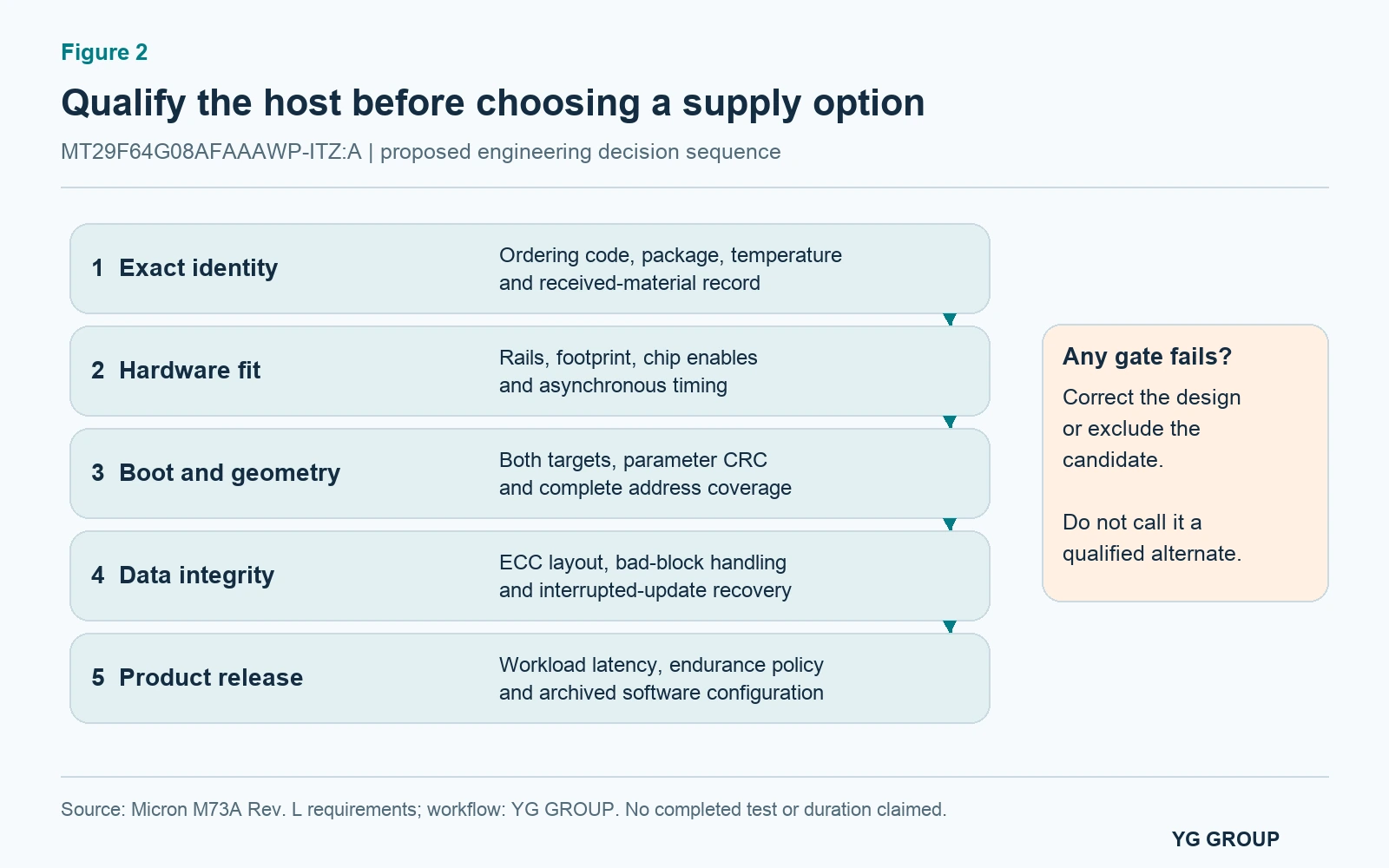
Table 5. A compact acceptance record for purchasing and engineering.
| Gate | Evidence to retain | Decision it supports |
|---|---|---|
| Identity and material | Full label, lot record and approved ordering description | Whether the offered material matches the request |
| Electrical and package fit | Rail, footprint, signal and temperature comparison | Whether existing hardware can use the candidate |
| Boot and enumeration | Cold-start logs, target geometry and parameter CRC results | Whether all required storage is reachable from startup |
| Data integrity | ECC layout, bad-block mapping and interrupted-write results | Whether the product preserves and recovers its data |
| Workload and release | Latency, erase-distribution and released software records | Whether the tested configuration satisfies the application |
Source: YG GROUP's proposed acceptance workflow, derived from Micron M73A power-up, organization, programming and error-management requirements. Consult Micron technical documents for the manufacturer's device requirements.
For incoming samples, retain the factory map before formatting and record the parameter data from each target. Keep the programming tool version with its configuration. If samples pass, archive the actual image and software build used rather than a note saying “tested.” This small discipline makes later lot checks reproducible and shortens the investigation when a different programming station behaves differently.
Procurement can then compare offers against a stable acceptance definition. Engineering can estimate a candidate's remaining work from a known gap instead of repeating a full investigation every time a quotation changes. Neither team has to pretend that a market forecast determines the precise timing of an individual order.
A good reason to retain MT29F64G08AFAAAWP-ITZ:A in a working design is the value of a correctly supported raw NAND implementation: validated startup, complete target access, appropriate ECC and a tested data-management policy. A good reason to change it is a documented product or sourcing benefit large enough to justify the required qualification.
Use NAND supply trends to decide when to review options; use host evidence to decide which options are usable. For this part, that means preserving the asynchronous TSOP identity, checking both targets and treating spare-area formatting as part of the product design. Those steps give a purchasing discussion something more valuable than a long list of similar names: a short list of configurations the product can actually depend on.
W38-38.pdf; Supplied source document; public access point: Micron technical-document search. The supplied revision was read in full; no copy of its pages is reproduced here.