
Beebee Chiang


27 views

| Picture | Part Number | Manufacturer | Stock | Action |
|---|---|---|---|---|
 | MP2451DT-LF-Z | Monolithic Power Systems | 3,370 | |
 | MP2451DT-LF | Monolithic Power Systems | 5,700 | |
 | MP2451DTLFZ | Monolithic Power Systems | 1,890 | |
| MP2451DJ-LF-Z | Monolithic Power Systems | 9,400 | |
| MP2451DJ-LF-P | Monolithic Power Systems | 3,630 |
No. It integrates the high-side MOSFET and requires an external catch diode. That diode's electrical and thermal behavior belongs in the complete design assessment.
No. It is the upper recommended input operating value. Evaluate the actual waveform and suitable margin; the separate 40 V absolute maximum is not a normal-operation target.
The cited Infineon commentary supplies no MPS order-code-specific stock, pricing, or lead-time evidence. Obtain those facts from a current, traceable offer and assess them separately from circuit suitability.
MP2451DT-LF-Z is an MPS non-synchronous step-down converter for a single output of 0.6 A or less. Its role is a small local power rail, where input conditions, light-load behavior, external components, and thermal margin determine suitability. Broad power-semiconductor growth does not establish demand or availability for this exact part. A useful buying decision starts with the rail specification and the complete SOT23-6 order code. MPS datasheet, pages 1–4 and 7.
Infineon's August 5, 2026 fiscal-third-quarter announcement described AI data-centre power supplies as its leading growth driver, grid investment as another source of momentum, and automotive orders as improving. The reporting period ended June 30, 2026. This is one manufacturer's market commentary, not an MPS order-book disclosure or a universal forecast for every power IC. Infineon Q3 FY2026 announcement.
The distinction matters when a general “power demand” discussion becomes a component-buying decision. Different end markets, converter functions, qualification requirements, and board programs can create different demand patterns. The cited update does not support treating automotive demand as uniformly weak, nor does it establish that every small regulator is benefiting equally from AI infrastructure spending.
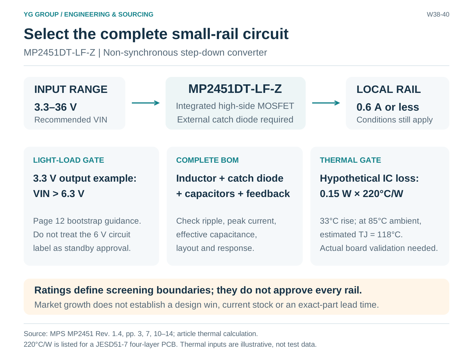
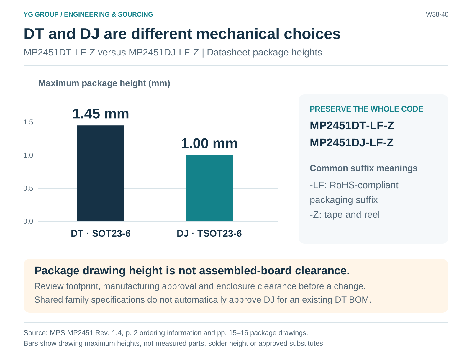
**Figure 1. Select the complete small-rail circuit.** YG Group synthesis of MPS MP2451 Rev. 1.4. Input and current figures are screening limits with application conditions. The 3.3 V light-load example preserves the page-12 VIN > 6.3 V guidance; it does not certify the page-13 6 V corner. The 118°C thermal estimate uses hypothetical 0.15 W IC loss and 85°C ambient with the listed board-conditioned 220°C/W value. Sources: [supporting source 1](https://www.monolithicpower.com/en/documentview/productdocument/index/version/2/document_type/Datasheet/lang/en/sku/MP2451/). **Figure 2. DT and DJ are different mechanical choices.** Package-drawing maximum heights from MPS MP2451 Rev. 1.4, compiled by YG Group. These are neither measured heights nor assembled-board clearance limits. Changing DT to DJ still needs the project’s mechanical, manufacturing and BOM review; common suffix meanings do not imply substitution approval. Sources: [supporting source 1](https://www.monolithicpower.com/en/documentview/productdocument/index/version/2/document_type/Datasheet/lang/en/sku/MP2451/).MP2451DT-LF-Z provides a concrete example at the small-rail end of the discussion. A control board may need a modest regulated supply while the system it belongs to handles much greater power. Selecting that local supply is a different task from choosing a GPU core power stage, a traction inverter, or a rack distribution architecture. No use in a named AI platform is claimed here.
The MP2451 integrates its high-side power MOSFET and uses current-mode control. It is non-synchronous, so the external Schottky catch diode is part of the power path. The design also requires an inductor, input/output capacitors, bootstrap capacitor, and the relevant feedback network. A small six-pin IC does not represent the whole solution's area or cost. MPS datasheet, Pin Functions and Operation.
Its recommended input range is 3.3–36 V and its stated output range is 0.8 V to 0.8 × VIN. These outer limits are useful initial filters, but they do not make every combination of input, output, and load equally suitable. The 40 V absolute-maximum VIN rating is a stress boundary, not a recommended input operating point. MPS datasheet, Recommended Operating Conditions.
The 0.6 A output capability must be assessed with inductor ripple, thermal behavior, and the actual operating conditions. The electrical table's 1.0 A typical current-limit entry concerns the switch-current limit; it does not turn the converter into a guaranteed 1 A output supply. MPS datasheet, Electrical Characteristics and inductor selection.
This is where a practical procurement comparison starts. Compare the complete approved circuit and the work needed to validate it, rather than ranking ICs by input-voltage range and unit price alone.
The MP2451's nominal switching frequency is 2 MHz, with a specified oscillator range of 1.6–2.4 MHz under the electrical table's conditions. At light load it enters pulse-skipping operation to reduce switching losses. The resulting operating mode matters for a rail that spends much of its life in standby. MPS datasheet, pages 4 and 7–8.
The bootstrap supply creates a particularly useful selection check. Page 12 states that, at no load or light load, VIN − VOUT should exceed 3 V to maintain adequate bootstrap voltage under the described conditions. It gives a 3.3 V output example requiring VIN above 6.3 V. The same section discusses an external bootstrap diode and recommends it for specified low-input/high-duty cases, including VOUT/VIN above 65%. MPS datasheet, External Bootstrap Diode.
Read that guidance alongside the typical circuits. Figure 3 labels its 3.3 V output circuit with a 6–24 V input range, while the preceding light-load guidance implies more than 6.3 V for its stated no-load/light-load condition. The figure's lower number should therefore not be used as a blanket assurance of 3.3 V regulation at a 6 V input in standby. Confirm the intended operating mode, bootstrap implementation, and minimum-input requirement with MPS and board measurements before approving that corner. MPS datasheet, Figure 3.
This is a concrete reason to define load states before choosing the regulator. A design that appears suitable at its normal operating load may need a different bootstrap arrangement, input threshold, or converter choice when its downstream controller sleeps. The article does not certify either a 6 V corner or an external-diode implementation.
The datasheet's feedback relation is VOUT = VFB × (1 + R1/R2). It recommends choosing the upper resistor near 124 kΩ and provides starting combinations for common output voltages. The feedback reference is nominally described as 0.8 V, while the electrical table lists its tested limits and a 0.794 V typical value. Use the limits and resistor tolerances for an accuracy budget, rather than treating a nominal equation as guaranteed output accuracy. MPS datasheet, pages 4 and 10.
Inductor selection must account for saturation current, ripple, resistance, and size. The manufacturer's equations calculate ripple and peak current from VIN, VOUT, switching frequency, and inductance. The peak, rather than only the average load current, must fit the switch and inductor limits. The named inductors in the datasheet are reference examples; their presence does not establish current availability or approval for a different rail.
The output capacitor and feedback/compensation components also affect the regulation response. The datasheet supplies typical component combinations and explains that capacitor characteristics affect stability. Internal compensation should not be interpreted as immunity to changes in the inductor, effective output capacitance, ESR, or layout. MPS datasheet, capacitor and compensation guidance.
| Decision area | Evidence needed for the actual rail | Procurement implication |
|---|---|---|
| Input envelope | Normal range, dips, overshoot, required margin | Do not select solely from a nominal “24 V” bus label |
| Output and load states | Voltage tolerance, startup demand, peak/steady/standby loads | Check both load capability and light-load headroom |
| Power-path components | Approved inductor, catch diode, capacitor ratings and tolerances | Compare the full BOM and qualified alternatives |
| Control and startup | EN drive, power order, output rise and restart behavior | Retain the circuit assumptions behind approval |
| Noise and response | Ripple, transient response, pulse-skipping behavior, EMI evidence | A typical efficiency curve does not replace validation |
| Thermal/mechanical fit | Actual dissipation, copper, environment, package drawing | A small package still needs thermal and assembly margin |
Table 1: Proposed rail-approval record, compiled by YG Group from the MPS operating, component-selection, and layout guidance. This is an engineering decision aid, not a completed board test or a manufacturer-mandated procurement form.
The recommended operating junction-temperature range ends at 125°C. The datasheet lists 220°C/W junction-to-ambient thermal resistance for both package options, measured on a JESD51-7 four-layer PCB. It also discusses thermal shutdown. That protection mechanism is not an acceptable normal operating target. MPS datasheet, page 3 and Thermal Shutdown.
For illustration, assume the IC itself dissipates 0.15 W and apply the listed 220°C/W value as a preliminary estimate. The calculated temperature rise is 33°C. At an assumed 85°C ambient, that gives 118°C junction temperature—only 7°C below the recommended upper boundary. These are hypothetical inputs, not measured MP2451 performance or an approved design margin.
Determine actual IC loss and board thermal behavior before using that estimate for approval. Total converter loss includes external diode and inductor dissipation, so assigning all system loss to the IC can also mislead. Conversely, nearby hot components can raise the local environment beyond the assumed ambient. Verify the operating extremes using the real PCB and enclosure.
The layout section reinforces the link: keep the switching-current loop compact, place input bypass capacitors close to VIN, keep feedback connections short, and route SW away from sensitive feedback circuitry. These are functional design requirements that belong in a cost comparison when a proposed component change would force layout or validation work. MPS datasheet, PCB Layout Guide.
The primary and secondary are close electrical relatives, but their package codes matter.
| Exact order code | Datasheet package | Maximum package height shown | Selection consequence |
|---|---|---|---|
| MP2451DT-LF-Z | SOT23-6 | 1.45 mm | Primary package; use its drawing and approved assembly record |
| MP2451DJ-LF-Z | TSOT23-6 | 1.00 mm | Lower-profile option; review mechanical and manufacturing approval |
Table 2: Package distinction, compiled by YG Group from MPS ordering information and package drawings, pages 2, 15, and 16. The figures are maximum package heights from the drawings, not assembled-board clearance guarantees.
The ordering instructions identify -Z as tape-and-reel and -LF as the RoHS-compliant packaging suffix. The official MPS product page also lists both complete order codes. Preserve that identity across the BOM, quotation, manufacturer label, and incoming-inspection record. Shared family specifications and similar land patterns do not constitute automatic approval to substitute DJ for DT.
The datasheet mentions automotive systems as an application category. That alone does not establish a specific automotive qualification for the offered order code or approval of a customer's vehicle design. Qualification evidence, where required, remains a separate purchasing condition.
MP2451DT-LF-Z is worth evaluating where a small local rail fits its input, output-current, component, and thermal requirements. The decisive work is checking the load profile, bootstrap headroom, complete BOM, layout, and exact package. Market developments can explain why a program is expanding; the rail specification and validation evidence determine whether this converter belongs in that program.
Author: Beebee Chiang