
Alice Chen




Get the latest tech insights
© 2026 YG GROUP. All rights reserved.
| Picture | Part Number | Manufacturer | Stock | Action |
|---|---|---|---|---|
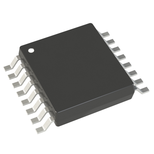 | ADG1408YRUZ-REEL7 | Analog Devices | 3,450 | |
| ADG1408YRUZ | Analog Devices | 2,410 |
It selects one of eight channels to the common terminal. EN low turns all channels off. It does not provide eight simultaneous independent routes.
No. It is a typical value in the ±15 V specification. Use the applicable supply table and temperature column, including the maximum and test conditions needed for the error budget.
No. The cited market forecast concerns global equipment sales. Availability of this exact order code requires separate, current supplier evidence.
ADG1408YRUZ-REEL7 is an Analog Devices eight-channel analog multiplexer in a 16-lead TSSOP package. It connects one selected channel to a common terminal and is documented for automatic test equipment. Evaluating it for a test signal path requires more than its low on-resistance headline: supply range, leakage, switching transients, settling, and exact ordering identity all affect whether the route preserves the measurement. Market growth provides context, while the circuit determines suitability. ADI datasheet, pages 1, 10, and 19.
SEMI's July 14, 2026 outlook forecasts global semiconductor test-equipment sales of $15.3 billion in 2026, up 31.0% from the previous year. This is a worldwide equipment-sales forecast, not a count of installed testers or an order forecast for ADG1408YRUZ-REEL7. SEMI mid-year equipment forecast.
For a team expanding or maintaining test capability, the useful component question is which signals need routing and what errors that routing may introduce. ADI explicitly lists automatic test equipment among the family's applications. That supports evaluating the part for this function; it does not show that a named tester uses it or that rising equipment investment will create a shortage of this order code. .
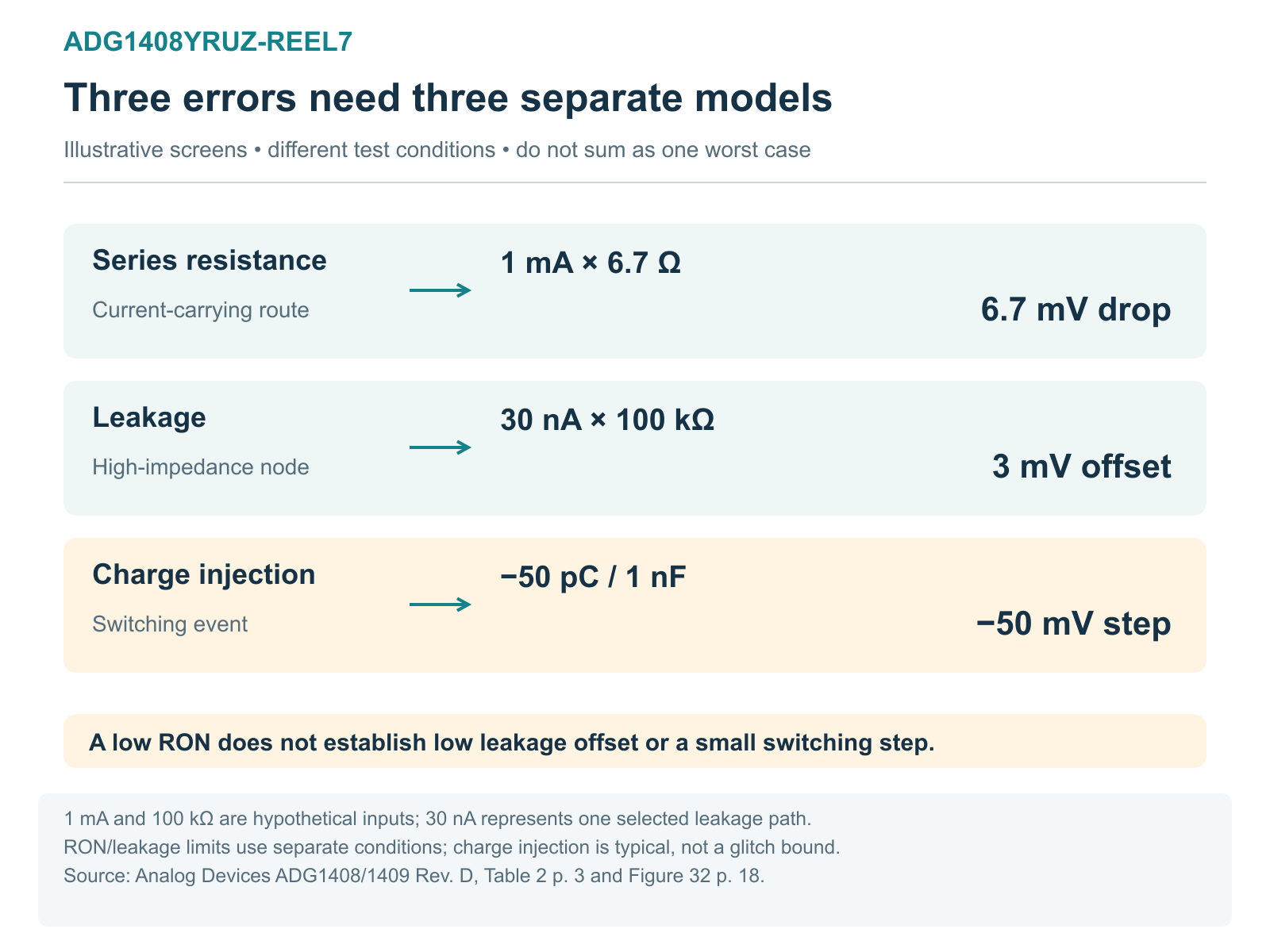
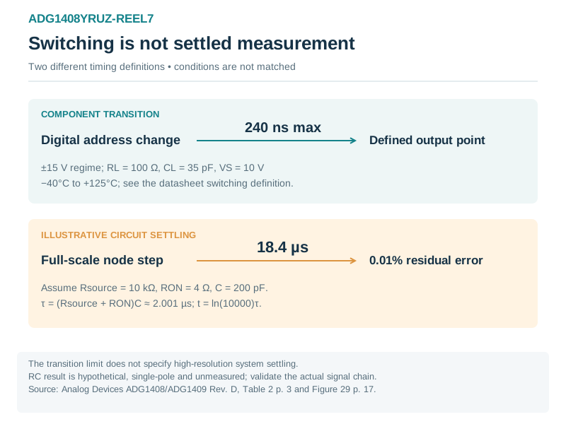
**Figure 1. ADG1408YRUZ-REEL7 static and transient errors need separate models.** Separate illustrative error screens, not a simultaneous worst-case sum. Series drop uses an assumed 1 mA and 6.7 Ω maximum RON from the ±15 V regime at reduced ±13.5 V supplies, VS = ±10 V, IS = −10 mA and −40°C to +125°C. Leakage uses one assumed 30 nA path through 100 kΩ; the cited full-temperature drain-off/on limit uses ±16.5 V supplies. Charge injection uses −50 pC typical at the ±15 V table’s VS = 0 V, RS = 0 Ω and CL = 1 nF condition, giving −50 mV by the defined test relation. None is a measured system error or a settled ADC-error guarantee. Sources: [supporting source 1](https://www.analog.com/media/en/technical-documentation/data-sheets/ADG1408_1409.pdf#page=3); [supporting source 2](https://www.analog.com/media/en/technical-documentation/data-sheets/ADG1408_1409.pdf#page=18). **Figure 2. ADG1408YRUZ-REEL7 switch transition versus measurement settling.** These are separate timing definitions under different conditions, not a matched performance comparison. ADG1408 transition time is 240 ns maximum over −40°C to +125°C in the cited ±15 V regime with RL = 100 Ω, CL = 35 pF and VS = 10 V. A hypothetical 10 kΩ source, 4 Ω switch and 200 pF node give τ ≈ 2.001 µs and 0.01% first-order settling in about 18.4 µs. This idealized calculation does not predict a complete instrument or a guaranteed device settling time. Sources: [supporting source 1](https://www.analog.com/media/en/technical-documentation/data-sheets/ADG1408_1409.pdf).Begin the routing specification with the signal's voltage range, source impedance, allowable current, accuracy target, channel-switching pattern, and required acquisition time. A low-impedance stimulus path and a high-impedance measurement node can need very different error budgets even when both use an eight-channel multiplexer.
ADG1408 is an eight-to-one single-ended multiplexer. Address inputs A0, A1, and A2 select the channel when EN is high; EN low switches every channel off. The S and D analog terminals can each serve as an input or output, so the route can be used bidirectionally within its electrical limits. This is not eight simultaneous signal outputs. ADI datasheet, Table 8 and Table 9.
The shared datasheet also covers ADG1409, a four-channel differential multiplexer. Its topology, pin assignments, and several electrical values differ. An ADG1409 row must not be copied into an ADG1408 design merely because both names appear on the cover.
The full primary order code ADG1408YRUZ-REEL7 and the close secondary ADG1408YRUZ are both directly listed in the ordering guide with the RU-16 TSSOP package and −40°C to +125°C temperature range. Retain the selected full code in the BOM and purchasing documents, and confirm the offered shipping presentation with the supplier. The ordering table establishes their common device/package grade; it does not identify the contents or handling history of a particular offered lot. ADI datasheet, Ordering Guide.
The TSSOP drawing has 0.65 mm lead pitch. The alternative LFCSP drawing in the same document belongs to a different package option; its exposed-pad instructions are not a TSSOP footprint requirement. Check the actual RU-16 drawing and pin mapping before approving a board or replacement purchase.
The datasheet provides separate electrical tables for ±15 V, +12 V single-supply, and ±5 V operation. The permitted analog signal range follows VSS to VDD; with the +12 V single-supply configuration, the range starts at ground. A negative input is not made permissible by the presence of a bipolar specification elsewhere in the document. ADI datasheet, Tables 2–4.
Supply choice changes the resistance budget. The frequently quoted 4 Ω is typical under the ±15 V specification. At +12 V single supply the listed typical on-resistance is 6 Ω, and at ±5 V it is 7 Ω. Maximum values also depend on temperature and the stated supply/signal conditions.
| Specification regime | Typical RON at +25°C | Maximum RON over −40°C to +125°C | Conditions attached to the maximum row |
|---|---|---|---|
| ±15 V | 4 Ω | 6.7 Ω | VDD = +13.5 V, VSS = −13.5 V; VS = ±10 V, IS = −10 mA |
| +12 V single supply | 6 Ω | 11.2 Ω | VDD = 10.8 V, VSS = 0 V; VS = 0–10 V, IS = −10 mA |
| ±5 V | 7 Ω | 12 Ω | VDD = +4.5 V, VSS = −4.5 V; VS = ±4.5 V, IS = −10 mA |
Table 1: Supply-specific resistance screening, compiled by YG Group from ADI Tables 2–4. Typical values use the nominal supply conditions of their respective tables; maximum values retain the explicit reduced-supply test conditions. Values are not interchangeable across regimes.
The continuous-current limit also changes. For ADG1408 under the ±15 V regime's stated reduced-supply condition, Table 5 lists 190 mA at 25°C, 105 mA at 85°C, and 50 mA at 125°C. The 190 mA headline is therefore not a full-temperature allowance. Keep both the current limit and measurement-error requirement in the selection record. ADI datasheet, Table 5.
On-resistance creates an I × R voltage drop in a current-carrying route. Resistance variation with signal level and temperature can make a single calibration insufficient. The datasheet distinguishes resistance, channel-to-channel matching, and flatness for this reason; they answer different measurement questions. ADI datasheet, Tables 2–4 and Terminology.
Leakage matters differently. A small leakage current can create a meaningful offset when it flows through a high effective source resistance. Do not assume that an excellent low-resistance result also guarantees a good high-impedance measurement. The leakage tables distinguish source-off, drain-off, and on-channel leakage, and give separate temperature limits.
Switching adds a third issue: charge injection. Figure 32 defines QINJ = CL × ΔVOUT. At the ±15 V table's VS = 0 V, RS = 0 Ω, CL = 1 nF condition, the listed charge injection is −50 pC typical. That corresponds to a −50 mV step in that specified test relation. It is a typical switching disturbance, not a maximum error bound for every signal voltage or node capacitance. ADI datasheet, Table 2 and Figure 32.
| Screening question | Illustrative calculation | What the calculation does not establish |
|---|---|---|
| What could series resistance add? | Assume 1 mA through 6.7 Ω: 6.7 mV drop | The actual RON at every current, signal, or supply condition |
| What could leakage do to a high-impedance node? | Assume one 30 nA contribution through 100 kΩ: 3 mV offset | The signed sum of all switch, board, receiver, and protection leakage paths |
| How large is the specified charge-injection step? | −50 pC / 1 nF = −50 mV | A guaranteed glitch bound or settled ADC error |
Table 2: Illustrative error-budget arithmetic, compiled by YG Group. Parameter context: ADI Table 2 gives 6.7 Ω maximum over the full temperature range under its RON conditions, 30 nA maximum magnitude for the specified full-temperature drain-off/on leakage rows at ±16.5 V supplies, and −50 pC typical under its charge-injection conditions. The current and 100 kΩ resistance are hypothetical design inputs. These rows are separate screens, not a combined worst-case simulation.
The next step is to identify the actual path for each error. A leakage current that returns elsewhere does not necessarily flow through the same 100 kΩ. A buffer changes the impedance and dynamic response. Fixture contamination, receiver bias, protection devices, and cable capacitance belong in the board-level budget. The table is a starting method, not a claim that this device will create those three errors simultaneously in a particular tester.
At the ±15 V specification, ADG1408 has a typical transition time of 140 ns and a maximum of 240 ns over −40°C to +125°C, with RL = 100 Ω, CL = 35 pF, and VS = 10 V. Figure 29 measures from the digital address transition to the defined output point. That is not the time for a high-resolution measurement system to settle to its final accuracy. ADI datasheet, Table 2 and Figure 29.
A simple analytical example makes the distinction clear. Assume a first-order node with 10 kΩ source resistance, 4 Ω switch resistance, and 200 pF total effective capacitance. Its time constant is approximately 2.001 µs. Settling to 0.01% of a step takes about 9.21 time constants, or 18.4 µs, in this idealized model. This is a calculation using hypothetical circuit values, not a guaranteed ADG1408 settling specification. An amplifier, ADC input network, multiple poles, charge injection, or cable can require a different model and longer validation interval.
The device's break-before-make behavior prevents overlap between selected channels under its specified switching definition. It does not make switching glitch-free or remove the need to wait before sampling. Define acquisition timing from the system error target, and verify the most demanding channel-to-channel voltage step with the real source, fixture, buffer, and converter.
The ADG1408's 60 MHz typical −3 dB bandwidth belongs to the ±15 V table with RL = 50 Ω and CL = 5 pF. It is not an ADC sample-rate rating, and the corresponding +12 V and ±5 V tables list different bandwidths. The same discipline applies to the −70 dB typical off-isolation and crosstalk entries at 1 MHz: the source, loading, supply, and frequency matter. ADI datasheet, Tables 2–4 and Figures 33–35.
For a mixed signal test route, examine the operating frequency and the other channels' signal amplitudes. A sensitive low-level measurement can be affected by an unselected channel even when the selected path's insertion loss is acceptable. Layout, decoupling, connector arrangement, and fixture routing must be assessed with the complete instrument. The datasheet's frequency curves and test circuits describe how to interpret the component data; they do not constitute a completed isolation test for a new board.
Also check the unpowered state and fault exposure. Rev. D's maximum-ratings notes describe internal clamp diodes and voltage/current limits for analog and digital inputs. Those are stress boundaries, not evidence of powered-off protection or permission to drive an arbitrary tester signal into an unpowered part. ADI datasheet, Absolute Maximum Ratings.
For ADG1408YRUZ-REEL7, a useful approval record combines the full ordering code with the supply regime, signal limits, temperature range, error budget, and acquisition timing that were actually validated. Keep the RU-16 package drawing with the footprint revision and retain the supplier's traceability and shipping information separately.
ADG1408YRUZ is a closely related ordering entry with the same documented device grade and TSSOP package. Evaluate any purchasing change against the factory's approved presentation and handling requirements. Do not use a shared base name as authorization to switch to ADG1409 or to an LFCSP package. No current stock, lead time, price, or specific lot qualification is established in this article.
It selects one of eight channels to the common terminal. EN low turns all channels off. It does not provide eight simultaneous independent routes.
No. It is a typical value in the ±15 V specification. Use the applicable supply table and temperature column, including the maximum and test conditions needed for the error budget.
No. The cited market forecast concerns global equipment sales. Availability of this exact order code requires separate, current supplier evidence.
ADG1408YRUZ-REEL7 gives test-equipment engineers a documented eight-to-one routing option. Its suitability depends on preserving signal range, current limits, static accuracy, switching recovery, and isolation under the chosen supply conditions. Keep those requirements connected to the exact package and order code. That produces a component decision the team can validate, rather than one inferred from a market headline.
Author: Alice Chen