
Doris Lee




| Picture | Part Number | Manufacturer | Stock | Action |
|---|---|---|---|---|
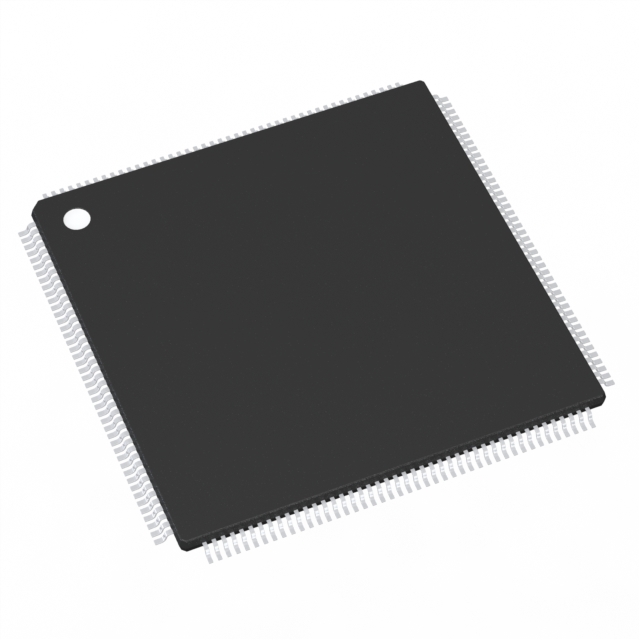 | XC2C256-7TQG144C | Xilinx | 7,220 | |
 | XC2C256-7VQG100I | Xilinx | 3,030 |
No. VCC and VCCIO have separate roles. DS094 specifies 1.7–1.9 V for the internal VCC supply; 3.3 V-class bank operation uses the separate VCCIO pins. Keep those nets distinct in the symbol and supply review. DS094, pp. 3,15
No. The TQ144 package provides 118 user I/O. Power, ground and JTAG occupy other package pins, and some user-I/O locations share global functions. Start with the package-specific map instead of assuming every lead can carry a user signal. DS094, pp. 11–15
No direct replacement is established. DS094 lists it as a 100-pin lead-free VQFP with 80 user I/O and an industrial ambient range of −40°C to +85°C. It differs from the 144-pin commercial target in footprint, available I/O and temperature designation. A design using it requires a separate pin allocation and board review. DS094, pp. 16–17
No. Match guaranteed VOH/VOL to the receiving VIH/VIL limits for each direction and load. The nominal rail helps select the relevant specifications, but it does not prove the available logic margin. DS094 supplies separate electrical tables for the supported standards. DS094, pp. 4–6
By Doris Lee | YG Group
XC2C256-7TQG144C is a Xilinx CoolRunner-II complex programmable logic device (CPLD) with 256 macrocells, a 144-pin lead-free TQFP package and 118 user I/O. Its two I/O banks let a board use different interface supplies while the internal logic runs from a separate 1.8 V-class rail. A workable bank plan must connect package pins, output voltages, input thresholds and timing constraints. This guide turns those requirements into a review sequence for an existing mixed-voltage board.
The technical reference is Xilinx DS094, version 3.2, dated March 8, 2007. Its ordering table names the exact part. The recommendations below concern electrical integration of a documented device; they do not establish current availability or a production status. Xilinx DS094, pp. 1,16–17
The suffix determines which package drawing, temperature range and timing column apply. XC2C256-7TQG144C is the -7 speed grade, in a 144-pin lead-free Thin Quad Flat Pack, for the commercial ambient range of 0°C to +70°C. The package body is 20 mm × 20 mm with 0.5 mm lead spacing. The 144 package pins include supplies, grounds and JTAG; the user-I/O count is 118. Xilinx DS094, pp. 15–17
*Figure 1. Illustrative supply allocation for XC2C256-7TQG144C. The bank voltages are one possible LVCMOS assignment, not a complete circuit. Core and bank pin numbers come from the TQ144 column; JTAG has a separate supply. Source: Xilinx DS094 v3.2, pp. 2–3 and 15. Diagram: YG Group. [Read DS094](https://docs.amd.com/v/u/en-US/ds094).* *Figure 2. Proposed per-net review sequence. Check each signal direction separately; bank voltage alone does not establish input margin, output loading or timing closure. This is a design-review framework, not a measured result. Source basis: Xilinx DS094 v3.2, pp. 4–9 and 11–15. Diagram: YG Group. [Read DS094](https://docs.amd.com/v/u/en-US/ds094).*It is not the -7 single-product-term maximum in the AC table. That column gives 6.7 ns for TPD1, with a separate 7.5 ns OR-array value. The design still needs its actual path and applicable I/O timing settings checked. DS094, pp. 1,6–9
That distinction matters when reviewing an inherited symbol. A symbol with 144 signal pins is already wrong, even before considering bank assignments. Likewise, the front-page 5.7 ns headline is not a blanket delay for this -7 ordering code. Use the -7 column and the implemented path, including relevant I/O adders, when building a timing budget.
Keep the full ordering code in the schematic part properties, bill of materials and programming release record. A shortened “XC2C256” label can identify the logic family, but it cannot identify the board footprint or the timing grade used to approve that board.
XC2C256 separates its internal supply, its two I/O-bank supplies and the JTAG supply. The core rail must stay within 1.7–1.9 V under recommended operating conditions; selecting 3.3 V outputs does not make the core a 3.3 V device. Xilinx DS094, p. 3
| Supply role | Recommended operating range | TQ144 package pins | Review consequence |
|---|---|---|---|
| Internal VCC | 1.7–1.9 V | 1, 37, 84 | Check the core rail independently of the I/O rails |
| VCCIO1 | 3.0–3.6 V, 2.3–2.7 V, 1.7–1.9 V or 1.4–1.6 V, according to the selected nominal bank supply | 27, 55, 73, 93 | Connect all Bank 1 supply pins to its chosen rail |
| VCCIO2 | The same four supported operating ranges | 109, 127, 141 | Connect all Bank 2 supply pins to its chosen rail |
| VCCAUX for JTAG | 1.7–3.6 V | 8 | Review the programming interface and its voltage separately |
Table 1. Recommended supplies and exact TQ144 power-pin mapping. The four VCCIO ranges correspond respectively to nominal 3.3 V, 2.5 V, 1.8 V and 1.5 V operation; they are alternatives, not a continuous permitted operating range. Source: Xilinx DS094, pp. 3,15.
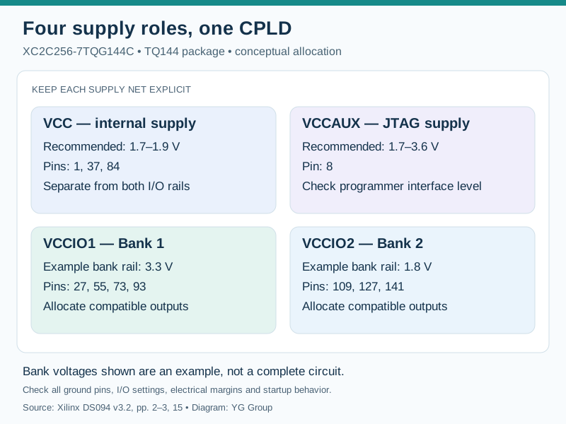
For example, a design may allocate 3.3 V outputs to one bank and 1.8 V outputs to the other. This is a useful starting point for control logic between two voltage domains. It remains an illustrative allocation: the design must also implement the intended signal directions, correct I/O settings and acceptable timing. The bank supply is shared by the bank’s output drivers; changing it is a board-level change affecting the attached outputs.
Treat the ground network and local supply integrity as part of the same review. Record regulator tolerance and expected rail variation at the device, then verify the result on the actual board. Absolute maximum ratings describe stress limits; they are not alternative design targets for a rail that misses its recommended range.
Use the TQ144 column of the pin-description table to identify each signal’s bank. Do not infer bank membership from a convenient group of adjacent pins or copy the map from another XC2C256 package. The datasheet provides bank membership per function-block/macrocell entry, followed by a separate power and JTAG table. Xilinx DS094, pp. 11–15
Global-function pins deserve an early reservation pass. For TQ144, GCK0, GCK1 and GCK2 appear at pins 30, 32 and 38 in Bank 1. GSR appears at pin 143 in Bank 2; the global output-enable functions also have specified locations. These shared pins can serve general I/O where documented, but assigning them that way may consume a resource the logic design later needs. Review the required clocks, reset and output enables before using all convenient pins for ordinary signals. Xilinx DS094, pp. 11–14
Build a compact worksheet with one row per external net: signal name, direction, package pin, bank, bank rail, I/O standard, peer device and required special function. Compare it with both the schematic and the fitted design report. This catches a common review gap: the HDL names the correct signal, but the physical pin or selected electrical standard belongs to the wrong interface plan.
An acceptable rail assignment does not by itself prove that two devices communicate reliably. For each direction, compare the driver’s guaranteed output levels at the relevant load with the receiver’s specified input thresholds. Leave margin for the actual electrical environment instead of treating two nominal voltage labels as a compatibility test.
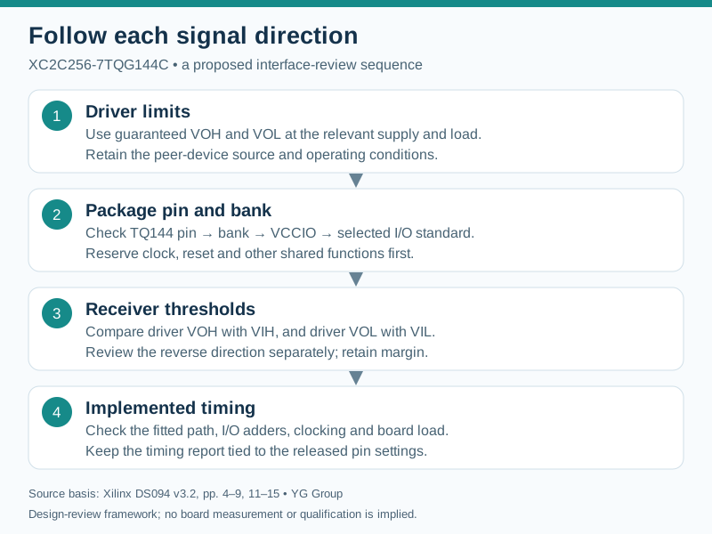
The calculation starts with two separate checks:
Use values from compatible operating and loading conditions. A positive DC difference is a necessary check for the selected interface; it is not a substitute for signal-integrity or timing verification. Trace drops, noise and switching behavior still need attention.
DS094’s 3.3 V LVCMOS/LVTTL table specifies a 2.0 V minimum high input level. Its 1.8 V LVCMOS output table specifies a minimum VOH of VCCIO − 0.45 V at IOH = −8 mA and VCCIO = 1.7 V. That produces a 1.25 V guaranteed minimum under that test condition, which cannot establish a high level for a receiver requiring 2.0 V. This example explains why connecting a lower-voltage output directly to a higher-threshold input needs an actual margin calculation. It is not a prediction of the typical output voltage. Xilinx DS094, p. 4
Do the reverse direction independently. Input survival limits, logic recognition and output-drive capability answer different questions. A voltage that does not damage an input is not automatically the right guaranteed operating point for the chosen standard.
LVCMOS15 requires Schmitt-trigger inputs in DS094. Therefore a 1.5 V interface review must check that configuration as well as its supply range and hysteresis thresholds. Simply choosing a 1.5 V rail leaves an essential input setting unresolved. Xilinx DS094, pp. 2,4–5
SSTL and HSTL need a different review from ordinary LVCMOS. The datasheet lists reference-voltage and termination requirements for these standards. When they are part of a design, account for VREF allocation, its required behavior and the board termination before finalizing pins. The summary table is not a complete reference-interface implementation recipe. For an LVCMOS-only board, avoid adding those requirements merely because the family supports them. Xilinx DS094, pp. 2,5–6
This distinction keeps the pin plan practical. Reserve only the resources needed by the actual electrical standards, but make those reservations before the board layout becomes expensive to change.
For the -7 grade, DS094 lists a maximum single-product-term propagation delay TPD1 of 6.7 ns and an OR-array propagation delay TPD2 of 7.5 ns in its AC table. The internal timing tables also list separate delays for I/O standards, hysteresis and slew-rate choices. Those settings cannot be ignored when changing a bank or input mode. Xilinx DS094, pp. 6–9
Use the implemented path and timing model, rather than adding unrelated table entries into a universal delay figure. For a registered interface, capture the external driver’s clock-to-output, board delay, CPLD setup/hold requirement and clock relationship. For an output path, include the receiving device’s requirement and the output loading assumed in the analysis.
Keep the fitted timing report tied to the exact pin constraints and electrical settings used for production. Re-run the check after moving a signal between banks, changing a Schmitt input or choosing a different slew option. A previously passing report describes its original implementation, not every later pin assignment.
A useful release record links the schematic, pin worksheet, fitted design and board checks. It lets a second engineer reproduce the reasoning behind each mixed-voltage connection.
| Review item | Evidence to retain | Reason to return to the design |
|---|---|---|
| Exact part and footprint | Full ordering code, TQ144 symbol and footprint review | Package or speed grade differs from the approved build |
| Supply assignment | All VCC, VCCIO1, VCCIO2, VCCAUX and ground connections | A bank rail or supply pin has no defined connection |
| Electrical interface | Per-direction level and loading checks | Guaranteed driver levels do not meet receiver thresholds |
| Configuration | Pin assignments and I/O-standard settings from the fitted design | Schematic and implementation disagree |
| Timing and startup | Constrained timing report and a board validation procedure | A required path or startup condition is untested |
Table 2. Suggested engineering review record compiled by YG Group from the device’s documented supply, pin and timing constraints. It is a proposed workflow, not a claim that a specific board has passed validation.
For an existing board, capture startup rail behavior and external signal activity before declaring the integration complete. Document what the attached devices do while supplies rise and while outputs are disabled. A normal steady-state trace cannot establish the behavior of every power transition. Detailed sequencing and programming requirements should be checked against the applicable implementation documentation rather than inferred from the nominal voltages alone.
A reliable XC2C256-7TQG144C review connects four things: the exact TQ144 pin, its bank supply, the signal’s electrical requirements and its implemented timing. Preserve that relationship in a per-net worksheet and a matching fitted report. It makes a mixed-voltage design easier to review and gives later maintenance work a concrete basis for evaluating a changed rail, pin assignment or device option.