
Evan Huang




Get the latest tech insights
© 2026 YG GROUP. All rights reserved.
| Picture | Part Number | Manufacturer | Stock | Action |
|---|---|---|---|---|
 | W25Q16JVSSIQ | Winbond | 5,930 | |
 | W25Q16JVSSIQ TR | Winbond | 3,850 | |
| W25Q16JVSSIQG | Winbond | 9,370 | |
| W25Q16JVSNIQ | Winbond | 2,050 | |
| W25Q16JVSNIQ TR | Winbond | 7,270 |
No. The IQ ordering option fixes QE at 1. Read Status Register-2 when diagnosing the interface, then configure the host for the selected Quad command. Do not infer the IQ behavior from a different JV suffix that has a programmable QE setting.
Yes. Winbond documents Standard, Dual and Quad SPI operation with QE=1. A 03h read remains useful as a simpler baseline. The additional data-pin functions must still be respected when reviewing the board connections.
No. It demonstrates a particular command and response path. It does not exercise the boot address, image contents, Quad data lines or the complete intended timing. Compare a known image region using both the baseline and target read protocols.
The commands use different address widths and pre-data phases. Verify the EBh four-line address, mode byte set to Fxh and four subsequent dummy clocks. Also check aligned starting addresses, wrap configuration and all four I/O connections before attributing the failure to clock frequency.
By Evan Huang | YG Group
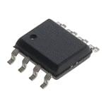
W25Q16JVSSIQ is Winbond's 16 Mbit serial NOR flash in an 8-pin, 208-mil SOIC package. Its Q option fixes Quad Enable at 1, so reliable boot depends on matching the host's command format, wiring and startup timing rather than programming QE. This guide explains how to establish a basic SPI read, configure Quad transfers and test recovery without confusing Quad SPI with QPI or changing unrelated protection settings.
The final letters matter to both firmware and board layout. Winbond's W25Q16JV Revision J datasheet explicitly lists W25Q16JVSSIQ, with SS identifying the 208-mil SOIC and I the -40°C to +85°C industrial temperature range. The Q option specifies QE fixed at 1. These are the applicable settings for this article; the wider family's other packages and temperature options do not change them. Winbond ordering information, printed pp.72-73.
It is a related IQ device, but SN identifies the 150-mil package while SS identifies the 208-mil package. Compare the package drawings and actual board requirements. Shared density and command family do not establish a direct mechanical or system replacement.
| Item | Verified value or behavior | Design consequence |
|---|---|---|
| Main array | 16 Mbit, or 2,097,152 bytes | Budget firmware and data partitions against 2 MiB, not 16 MB |
| Package | 8-pin SOIC, 208 mil (SS) | Check the actual footprint rather than assuming every SOIC-8 is interchangeable |
| Temperature | -40°C to +85°C (I) | Do not apply the J option's +105°C range |
| Supply | 2.7-3.6 V, with frequency-dependent limits | Select the read clock from the operating and AC tables |
| Quad Enable | Status Register-2 bit S9, fixed at 1 for IQ | Read it diagnostically; no QE-enable write is required |
| JEDEC identification | EF 40 15 for the IQ/JQ configuration | Useful communication check; not proof of package or lot authenticity |
Table 1. Exact-part interpretation and boot implications. Source: Winbond W25Q16JV Rev. J, printed pp.4, 14, 19, 57 and 72-73. Compiled by YG Group.
The related W25Q16JVSNIQ retains the IQ option but uses the narrower 150-mil SOIC. The common memory family makes it a useful comparison; the different package prevents a blanket footprint-replacement claim. Confirm the land pattern, assembly limits and complete design requirements before approving any substitution.
QE=1 enables the additional I/O pins, but it does not make every command a four-line transaction. W25Q16JVSSIQ accepts Standard, Dual and Quad SPI instructions. Its instruction table defines the width of each command, address and data phase separately. A controller's generic “Quad mode” switch is insufficient unless those phases match the selected opcode. Winbond Rev. J, printed pp.14 and 19-21.
In particular, this article's 6Bh and EBh commands send the opcode on one line. They are not 4-4-4 QPI transfers. The datasheet directs readers to a separate DTR document for QPI support; importing a QPI initialization sequence from another device changes the protocol assumptions and is not justified for this IQ guide.
Check all four data connections before moving beyond Standard SPI. For the SS package, pin 5 is IO0, pin 2 is IO1, pin 3 is IO2 and pin 7 is IO3. Pins 1 and 6 provide /CS and CLK, while pins 8 and 4 provide VCC and GND. With QE=1, the additional data functions replace /WP and /HOLD. A legacy board that ties these multifunction pins directly to supply or ground needs a circuit review before Quad transfers are attempted. The pin mapping and function changes are documented on printed pp.5 and 7; the board-review advice is an engineering consequence of that mapping.
A useful bring-up sequence proves communication and image contents before increasing protocol complexity. It is a proposed verification workflow, not a claim that every processor's boot ROM runs these steps.
9Fh for JEDEC ID, 05h for Status Register-1 and 35h for Status Register-2. Record the returned bytes, including BUSY and QE.03h. Compare the bytes with the intended image. An erased region returning FFh is a weak test because an undriven bus can appear similar.
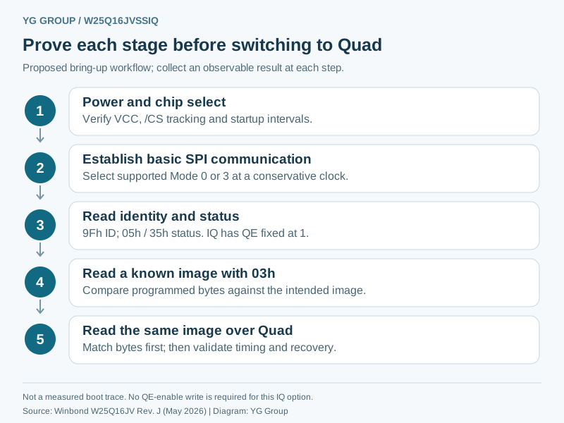
For startup, the datasheet lists a minimum 20 µs from VCC(min) to /CS low and a minimum 5 ms write-instruction delay. These are separate conditions, not interchangeable delays. The characterized power-cycle requirement also calls for VCC below the 0.8 V maximum VPWD threshold for at least 100 µs before a new power-up sequence. Measure the flash rail itself; a processor reset or a brief supply dip does not demonstrate that condition. Winbond Rev. J, printed pp.58-59.
If the processor's immutable boot ROM cannot produce the required transaction or startup behavior, later application firmware cannot repair the first failed fetch. Check the processor's boot documentation independently; no particular host has been qualified by this article.
6Bh and EBh both return data on four lines, but their address phases and waiting periods differ. Controller fields often express these details separately, so a correct opcode alone does not guarantee a correct read.
| Read instruction | Command / address / data widths | Address and pre-data sequence |
|---|---|---|
03h Read Data | 1-1-1 | 24-bit serial address; no dummy clocks |
0Bh Fast Read | 1-1-1 | 24-bit serial address, then 8 dummy clocks |
6Bh Fast Read Quad Output | 1-1-4 | 24-bit serial address, then 8 dummy clocks |
EBh Fast Read Quad I/O | 1-4-4 | 24-bit address over 4 lines, 8 mode bits over 4 lines, then 4 dummy clocks |
Table 2. Transaction definitions for this datasheet. For EBh, M7-M0 must be set to Fxh; the two mode clocks are additional to the four dummy clocks. Source: Winbond Rev. J, instruction table and read diagrams, printed pp.20-21 and 26-31.
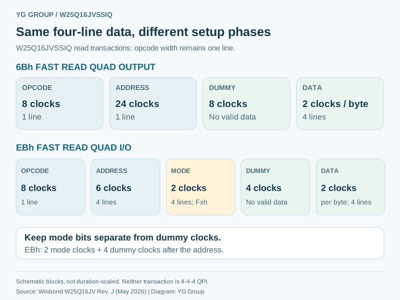
When a controller has an “alternate bytes” field, determine whether that field emits the EBh mode bits. If it instead groups mode and dummy phases under one configuration, verify the actual waveform and required transmitted values. Counting six clocks after the address without checking the first two clocks' contents misses this distinction.
The AC notes additionally require a four-byte-aligned starting address for Quad Read, with A1:A0=00. Make test regions and memory-mapped accesses comply with that condition. For linear reads, also confirm that burst wrap is disabled: 77h controls wrapping, W4=1 disables it, and that is the documented power-on/reset default. Previously enabled 8-, 16-, 32- or 64-byte wrapping can otherwise produce a repeating region that resembles an addressing fault. Winbond Rev. J, printed pp.31-32 and 63.
The 133 MHz family headline does not apply to every voltage or opcode. 03h is limited to 50 MHz. The other instructions have a stated maximum of 133 MHz at 3.0-3.6 V and 104 MHz at 2.7-3.0 V. Use the operating-range table together with the complete AC requirements, including clock shape, setup/hold timing and loading. Winbond Rev. J, printed pp.57 and 61-64.
The operating-range note also requires the read supply voltage to remain within ±10% of the programming (erase/write) voltage, while staying within the specified supply range. These limits describe the memory interface, not a guaranteed board frequency or boot time. Host sampling delay, interconnect loading, voltage margin and transaction overhead still affect a design. Increase frequency only after Standard and Quad reads agree at the initial setting, then validate the intended operating corners. Retain the configuration and captured failures so that a timing adjustment is not mistaken for a fix to a wrong opcode or address width.
An unconditional “write QE” routine creates unnecessary risk on this exact part. Status Register-2 also contains protection-related fields and one-time-programmable security-lock bits. Writing a constant register value copied from another driver can affect more than the intended setting. The IQ option's fixed QE does not justify modifying the remaining fields. Winbond Rev. J, printed pp.13-15 and 24-25.
Where the design deliberately changes a writable status field, distinguish the write paths. 06h enables a nonvolatile status write, with BUSY reporting the write cycle. 50h enables a volatile status write without setting WEL; BUSY stays zero during the register-refresh interval. The volatile values are lost on power-off or a flash software reset, restoring their nonvolatile counterparts. These mechanisms do not make the IQ option's fixed QE programmable. Apply the required timing and preserve unrelated writable fields under a reviewed configuration policy.
Recovery tests must also distinguish resetting the host from resetting the flash. The SS eight-pin package has no dedicated hardware /RESET pin; the datasheet's dedicated-reset description applies to other packages. The flash's software reset sequence is 66h followed by 99h; the datasheet specifies 30 µs maximum to the next instruction after reset. It warns that resetting during an active or suspended erase/program operation may corrupt affected data, and recommends checking BUSY and SUS first. A bootloader should therefore have an explicit recovery policy, not send reset commands indiscriminately. Winbond Rev. J, printed pp.9, 56 and 63.
For a flash intentionally placed in power-down with B9h, the documented wake command is ABh; other commands are ignored in that state. Observe the relevant release time before resuming transactions. Include cold start, host-only reset and wake from flash power-down as separate cases in the validation record.
For W25Q16JVSSIQ, record the full ordering code, supply conditions, host reset path and complete read transaction. Establish a known Standard SPI read, reproduce it over Quad SPI, then qualify clock margin and recovery behavior. That sequence makes a boot failure easier to localize while preserving protection settings and the exact IQ device assumptions.