
Ying Lin




| Picture | Part Number | Manufacturer | Stock | Action |
|---|---|---|---|---|
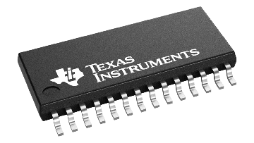 | TLC5941QPWPRQ1 | Texas Instruments | 4,540 | |
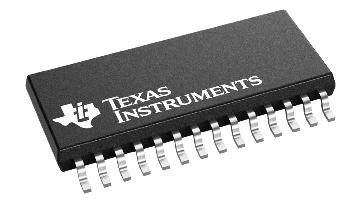 | TLC6C5712QPWPRQ1 | Texas Instruments | 5,400 |
Grayscale data determines channel on-time using 12-bit values and the GSCLK counter. Dot correction scales the current amplitude with a 6-bit value: IOUT = Imax × DC/63, from zero to the reference-set maximum. The TLC5941-Q1 recommended constant-current setting is at most 60 mA per channel. Combining these controls changes average current, but the lowest PWM codes remain subject to output timing errors.
The datasheet states that GS and DC register contents are unknown after power-on and must be programmed before outputs are enabled. It does not provide a persistent dot-correction EEPROM. Hold BLANK high during startup, set GS before DC as specified, and keep XLAT low while changing MODE. Store calibration in the controller or another suitable memory if it must survive loss of power.
New grayscale data should be latched at a frame boundary with BLANK high because it immediately replaces the active GS values. Dot-correction data can be latched with BLANK low, but conducting channels then change current immediately. Choosing to update DC during blanking avoids that current step. The first GS transfer after DC programming also requires an extra SCLK pulse after XLAT.
By: Ying Lin
The Texas Instruments TLC5941QPWPRQ1 is the HTSSOP-28 automotive ordering option for TLC5941-Q1, a 16-channel constant-current LED driver. Its 12-bit grayscale data controls how long each channel conducts; its 6-bit dot correction controls that channel’s current while on. Keeping those controls separate makes brightness updates predictable. The practical work is to initialize both registers, preserve the grayscale clock cycle and latch the next frame at the intended boundary, while budgeting the heat dissipated in the current sinks.
Grayscale PWM provides 4096 codes per output. Dot correction provides 64 current-setting codes, from zero through the programmed channel maximum. The global current reference resistor sets Imax; the per-channel DC value then scales it according to IOUTn = Imax × DCn/63. Dot correction is not a 33.3–100% trim range on this device. DC = 0 requests zero channel current and DC = 63 requests the full reference setting.
PWM changes the on-time without intentionally changing that current amplitude. For a simplified average-current estimate, multiply the on-state current by the PWM duty fraction. At the lowest grayscale codes, output timing errors mean the result is not perfectly proportional to the numerical code. Use the switching specifications and actual waveform to judge those codes rather than assuming that 12-bit data guarantees 12 bits of useful light output at every clock frequency.
Table 1: TLC5941-Q1 control domains and operating boundaries | Source: , recommended conditions and Sections 8–9 | Compiled by: YG GROUP.
*Figure 1: Functional separation of grayscale duty control and dot-correction current control. MODE selects the serial data destination; GSCLK and BLANK control the PWM counter independently of SCLK. Source: [TI TLC5941-Q1, SLDS165A](https://www.ti.com/lit/ds/symlink/tlc5941-q1.pdf), Sections 8–9; diagram: YG GROUP.* *Figure 2: Conceptual steady-state GS frame boundary, with a compressed 4096-clock cycle and XLAT during BLANK high. It is not a pulse-width specification or the first GS update after DC programming, which requires an additional SCLK after XLAT. Source: [TI TLC5941-Q1](https://www.ti.com/lit/ds/symlink/tlc5941-q1.pdf), Figures 17 and 22; timing illustration: YG GROUP.*A single grayscale clock period at 30 MHz is only about 33.3 ns. The datasheet’s on-time error can consume this small interval; its worked example shows an output that may not turn on. A lower clock rate or higher minimum usable code can provide more pulse-width margin. Verify actual LED current and brightness rather than equating every digital code with a guaranteed optical step.
| Function | Datasheet definition | Practical consequence |
|---|---|---|
| Logic supply VCC | 3.0–5.5 V | Check controller logic thresholds at the chosen rail |
| Maximum constant-current setting | 60 mA per channel | Do not import an 80 mA catalog-family setting |
| Grayscale register | 16 × 12 bits = 192 bits; MODE low | Separate duty-cycle data from current trim |
| Dot-correction register | 16 × 6 bits = 96 bits; MODE high | Current ratio is DC/63, with DC from 0 to 63 |
| SCLK and GSCLK | Up to 30 MHz each | Independent serial-transfer and grayscale clocks |
| BLANK high | All outputs off; grayscale counter reset | Establishes a defined frame boundary |
| OUT0–OUT15 voltage | Up to 17 V recommended | LED supply voltage alone does not equal sink voltage |
| Recommended junction temperature | −40°C to +125°C | Thermal error flag is not the normal operating limit |

The control pin is MODE, pin 6. MODE low selects grayscale data; MODE high selects dot correction. SCLK clocks SIN into the shift register on rising edges, MSB first. XLAT is a level-sensitive latch control: data reaches the selected register while XLAT is high and is held when XLAT is low. Keep SCLK and SIN stable during the high latch interval and respect the setup and hold requirements.
The selected part uses BLANK pin 2, XLAT pin 3, SCLK pin 4, SIN pin 5, XERR pin 23, SOUT pin 24, GSCLK pin 25, TEST pin 26, IREF pin 27 and VCC pin 28. TEST must be tied to VCC for correct dot-correction operation. Copying a VPRG-based schematic from a different LED driver would obscure the actual TLC5941-Q1 pin functions and make firmware review harder.
The power-on GS and DC contents are unknown. Keep BLANK high using the required pull-up while the controller starts. The datasheet instructs that initial GS programming precede DC programming, and XLAT remain low when MODE changes. Program defined data before allowing LED outputs to operate; this device does not provide a persistent dot-correction EEPROM that can replace initialization.
The grayscale counter starts from zero after BLANK. The first GSCLK rising edge increments it and turns on outputs with a nonzero GS value. Later rising edges increment the counter; an output turns off when the count reaches its programmed value. At FFFh, or 4095, the counter stops and outputs turn off. A conventional complete cycle uses 4096 GSCLK pulses before BLANK resets it; it does not freely roll over or count downward.
Shift new grayscale data during the active cycle if useful, but latch it at the end of the cycle with BLANK high. Loading new GS data mid-cycle immediately replaces the active values and can create an unexpected partial frame. An early BLANK truncates on-time and changes average brightness; it does not, by itself, prove that the code-to-brightness response reverses direction. Diagnose the captured waveform before attributing a particular visual artifact to a specific firmware race.

After changing from DC mode to GS mode, the first GS input cycle requires an additional SCLK pulse after XLAT. This transition-specific pulse is easy to omit when a routine treats every transfer as only 192 clocks. Keep it explicit in the state machine and in a logic-analyzer test. Subsequent steady-state GS transfers follow their normal timing sequence.
The datasheet permits a DC latch with BLANK low; that immediately changes the current of conducting outputs. Updating DC during an intentional blanking interval is therefore an application choice for avoiding a visible current step, rather than a claim that the device prohibits every active-frame DC update. Do not present that design choice as a universal hardware requirement.
At an assumed 5 MHz GSCLK, 4096 clocks take 819.2 µs. The complete frame period also includes the BLANK interval and any deliberate pauses, so its frequency is slightly below 1.221 kHz. For one device and an assumed 1 kHz update rate, the datasheet’s conservative 193-clocks-per-update sizing expression gives 193 kHz before allowing software, latch and blanking margin. Cascaded devices multiply the serial data budget.
The maximum 30 MHz GSCLK is not always the best dimming clock. The datasheet gives an example in which GS = 1 at 30 MHz produces a calculated negative on-time when the typical timing error is included, so that output may not turn on. Reducing GSCLK or raising the minimum usable code can improve low-brightness behavior. Check the actual LED current at the smallest intended codes and over temperature; a digital waveform alone does not show whether a short current pulse was delivered.
The current-setting relation is Imax = 31.5 × V(IREF)/R(IREF), using the application section’s typical 1.24 V reference value. An assumed 30 mA setting therefore needs about 1.30 kΩ. The recommended global setting is 5–60 mA; lower channel currents can be obtained through DC scaling. Reference voltage and current tolerance still apply.
Channel dissipation depends on the voltage actually remaining at each OUT pin, its current and its duty cycle. With an assumed 16 active channels, 30 mA each, 2.0 V at every OUT pin and 100% duty, the sink contribution alone is 0.96 W. Add logic supply power. The datasheet’s 36.7°C/W junction-to-ambient metric, measured under its stated board conditions, would correspond to about 35.2°C rise for that sink contribution alone. At 105°C ambient that simple estimate already reaches about 140.2°C, exceeding the recommended 125°C junction ceiling before logic power is included.
That calculation is a screening estimate, not a prediction of the real board temperature. It explains why the exposed thermal pad, copper, vias and LED voltage headroom matter. Use the package/layout guidance and characterize the intended board. Do not assume that a fixed number of vias creates a guaranteed thermal resistance, or that the thermal error flag makes operation above the recommended junction limit acceptable.
TLC6C5712QPWPRQ1 is a related TI automotive LED-driver candidate when diagnostic/control architecture matters. It has 12 channels, 8-bit dot correction and a 16-bit SPI interface, with output limits different from TLC5941-Q1. It is an architectural comparison, not a pin-compatible substitute or a higher-voltage way to reuse this design. Confirm the application’s channel count, sink voltage and control requirements against its own datasheet.
Check MODE, SCLK, XLAT, GSCLK and BLANK together during initialization, the first GS update after DC, and normal frames. Verify the required extra SCLK, defined startup data, and the intended latch boundary. Then measure LED current at low codes and at the worst thermal load. The reliable implementation keeps PWM timing, current calibration and thermal margin as separate, coordinated decisions.