
YG Group



21 views

| Picture | Part Number | Manufacturer | Stock | Action |
|---|---|---|---|---|
 | STM32H723VGH6 | STMicroelectronics | 6,910 |
No. A missing request, incorrect count, inaccessible memory region, disabled clock, transfer error or premature buffer reuse can produce a DMA symptom. Establish the selected master, actual linked addresses and transfer status first. Investigate cache visibility when the evidence supports that branch, using a defined ownership and maintenance policy rather than adding calls without a reproducible explanation.
MDMA has a documented TCM path in DS13313 pages 21 and 30. That capability must not be generalized to DMA1, DMA2, BDMA or every peripheral master. Identify the engine actually performing the transfer and verify its route to the chosen region. A successful CPU access to DTCM is not an independent proof of another master's reachability.
No. Within the complete ordering code, H selects TFBGA, while T selects LQFP. STM32H723VGH6 and STM32H723VGT6 therefore require different package and PCB checks even though V and G indicate matching connection-count and flash options. The temperature code 6 is separate from the package letter; preserving the complete suffix avoids confusing those fields.
Author: YG Group | Primary part: STM32H723VGH6 | Manufacturer: STMicroelectronics
STM32H723VGH6 is an STMicroelectronics Cortex-M7 microcontroller with a 32 KB data cache and a TFBGA100 package. Its memory system includes tightly coupled RAM, shared AXI memory and several DMA engines with different access paths. In industrial control or high-rate acquisition, a correct buffer address is only the first check: ownership and cache maintenance must also match the direction and lifetime of each transfer.
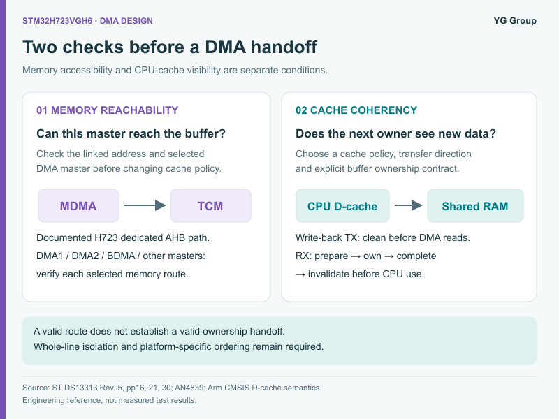
Check two independent conditions before blaming DMA: the selected DMA master must reach the chosen memory, and the next owner must see the current data. Cache maintenance cannot create a missing bus path. Moving a buffer into accessible RAM cannot by itself establish a correct ownership handoff.
No. The first is the total data-cache capacity stated for H723; the second is the granularity relevant to the Cortex-M7 maintenance operations discussed here. A 33-byte payload can occupy parts of two lines despite being tiny relative to the whole cache. Isolate both ends of shared buffers and validate the actual address-based maintenance implementation.
No. Volatile does not establish memory reachability, clean dirty cache contents, invalidate stale copies or transfer ownership safely. It addresses a different compiler-level concern. A correct driver contract also needs actual memory placement, effective attributes, direction-specific maintenance where applicable, completion synchronization and a rule preventing CPU access while DMA owns the buffer.
Not necessarily. Dedicated non-cacheable shared regions or validated per-buffer maintenance can be appropriate, depending on architecture and workload. Global disable changes system timing and has its own safe-transition requirements. Use it only as a controlled experiment or a justified design policy, not as proof that a specific cache operation or DMA configuration has been diagnosed correctly.
STM32H723VGH6 has 32 KB of instruction cache and 32 KB of data cache. Do not import an older STM32F7 or STM32H7 example's cache capacity or memory topology into this exact device. The ST DS13313 Revision 5 datasheet, dated May 2025, governs the H723 facts used here; a family application note provides principles, not a replacement memory map.
The complete suffix matters. In the ordering scheme, V identifies the 100-pin/ball option, G identifies 1024 KB of flash, H selects TFBGA and 6 identifies the −40°C to +85°C range. The exact ST STM32H723VGH6 ordering record confirms the product identity. A similarly named LQFP device is not the same footprint, even when the core and flash designation match.
| Suffix or resource | H723-specific meaning | Capacity or package | Boundary for this investigation |
|---|---|---|---|
| V / G / H / 6 | 100 connections / 1024 KB flash / TFBGA / −40°C to +85°C | Exact STM32H723VGH6 | Preserve the complete order in board and firmware records |
| Instruction cache | CPU instruction-side cache | 32 KB | Not an additional application SRAM allocation |
| Data cache | CPU data-side cache | 32 KB | Capacity differs from the 32-byte maintenance granularity |
| DTCM | Tightly coupled data memory | 128 KB | CPU and documented MDMA path; do not generalize to all masters |
| ITCM | Tightly coupled instruction memory | 64–256 KB, depending on allocation | Shared allocation changes available AXI SRAM |
| AXI SRAM | D1-domain system RAM | 128–320 KB, depending on allocation | Confirm the actual configuration, linker region and master access |
| Shared AXI/ITCM pool | Allocated to one use or the other | 192 KB, in 64 KB granules | Count once, not once in each memory category |
| Other internal SRAM | SRAM1, SRAM2 and SRAM4; backup RAM | 16 KB each; 4 KB backup | Different regions and domains require separate checks |
Table 1: Exact suffix and H723 memory-budget boundaries | Source: ST DS13313 Rev. 5, pages 1 and 21; ordering at printed page 230 | Compiled by: YG Group
The memory-budget arithmetic is a useful sanity check. The shared 192 KB pool cannot simultaneously provide its maximum contribution to both AXI SRAM and ITCM. If a linker script reserves a large ITCM section, revisit the AXI allocation rather than adding the two headline maxima. A project that assumes nonexistent RAM may fail for reasons that resemble data corruption but have nothing to do with cache maintenance.
Inspect the actual linked buffer address, not only its source declaration. A section attribute expresses intent; the linker map shows placement. Startup code, heap configuration and a library's internal allocations can introduce buffers outside the region reviewed by the application author. Record the address, length, alignment, lifetime and effective memory attributes of the actual object passed to the driver.
The distinction is especially important for high-rate acquisition. An application might keep critical CPU data in DTCM while arranging a peripheral transfer elsewhere. That is a design choice requiring a documented data handoff, not evidence that DTCM is universally wrong or universally reachable. The CPU can successfully read a location without proving that a different master has a route to it.
The exact device also has supply conditions that should not disappear behind a performance headline. DS13313 page 15 permits the 1.62 V supply floor with the specified external-supervisor and PDR_ON arrangement; otherwise its stated floor is 1.71 V. This is not a supply-design tutorial, but unstable power and reset conditions must be ruled out before interpreting intermittent transfers as a cache defect.
Family context is useful for understanding the wider Cortex-M7 ecosystem, but another device's overview does not establish H723 capacities, current inventory or memory reachability. Keep those questions tied to the exact part. The primary H723 document remains the authority for this article's device-specific architecture, even when a familiar family example appears to solve a similar problem.
Name the DMA master before asking whether “DMA can access RAM.” DS13313 describes MDMA, DMA1, DMA2 and BDMA as distinct instances, alongside specialized peripheral and graphics transfer engines. Their names are not interchangeable. A request router selects requests; it does not make every memory accessible to every master.
The H723 documentation explicitly gives MDMA a master AXI interface and a dedicated AHB path to Cortex-M7 TCM. DMA1 and DMA2 are described in D2, while BDMA is in D3. Those statements identify the architecture but are not a complete all-master/all-region permission matrix. Use the device's applicable reference documentation and the selected peripheral configuration to complete each row of the worksheet.
| Master or path | Documented starting point | Buffer region to record | Reachability evidence required | Remaining checks |
|---|---|---|---|---|
| CPU | Cortex-M7 cache, AXI and TCM interfaces | Actual address and effective MPU attributes | H723 memory map and linker output | A valid CPU access does not prove DMA access |
| MDMA | D1; AXI master and dedicated TCM AHB interface | Exact AXI or TCM source/destination | DS pages 21 and 30, then selected transfer configuration | Trigger, transfer width, address increment and completion |
| DMA1 | D2 dual-port DMA | Actual selected source and destination region | Master-to-region route in applicable H723 documentation | Peripheral request, clocks and transfer status |
| DMA2 | D2 dual-port DMA | Actual selected source and destination region | Independently verify the selected route | Do not substitute an MDMA capability |
| BDMA | D3 basic DMA | Actual selected source and destination region | Device-specific accessible-region check | Domain state, request selection and count units |
| Peripheral or graphics master | Engine-specific architecture | Data and any descriptors | Documentation for that engine and memory path | Descriptor ownership may differ from payload ownership |
Table 2: DMA-master access worksheet, not a universal reachability matrix | Source: ST DS13313 Rev. 5, pages 16, 21 and 30 | Compiled by: YG Group
A failed transfer can be separated into three observations: the request never arrived, the engine reported an access or configuration error, or the engine completed but the consumer saw unexpected data. These are different diagnostic branches. Capture peripheral status, DMA status and the final transfer count before changing cache policy. Otherwise a successful reconfiguration may hide the original cause without explaining it.
Memory access and data visibility are independent conditions. First establish whether the selected master can reach the actual buffer; then establish whether its owner sees current data. The documented H723 MDMA-to-TCM path answers a specific reachability question, not the coherency question for every transfer. A route that has not been verified for the selected master and memory region remains unresolved, even if a similar MCU's architecture appears familiar.
Once reachability is documented, identify all participating buffers. A communication stack can own a payload, a descriptor and a status structure separately. Reviewing only the payload may leave a cached descriptor holding an old ownership flag or an old length. The same questions apply to each object: who writes it, who reads it next, where it lives, and what event transfers ownership?
An industrial communication interface gives this ownership review a concrete application context. Its peripheral driver and application may use distinct payload and status objects, but that does not establish the H723's DMA route or imply that every peripheral uses the same memory arrangement. Document who owns each object at the boundary between the driver and the application.
Choose a policy for each shared buffer, then make ownership transfers explicit. In write-back memory, CPU-written data may need cleaning before another master reads them. After another master writes memory, the CPU may need invalidation before consuming the result. Cleaning and invalidating are different operations; neither is a substitute for preventing concurrent access.
ST AN4839 Rev. 2 explains the general distinction: cleaning writes dirty cache data back, while invalidation discards cached validity. Its older family capacities and F7 transfer example are not adopted as H723 architecture facts. The following ownership procedure is an engineering design pattern to validate on the actual firmware, not ready-to-paste driver code.
| Transfer situation | Owner before handoff | Memory policy | Required handoff concept | Hazard to exclude |
|---|---|---|---|---|
| CPU-produced transmit payload | CPU | Cacheable write-back | Finish CPU writes; clean the complete owned range; complete required ordering; then start DMA | DMA reads old memory while newer bytes remain dirty in cache |
| DMA-produced receive payload | CPU prepares, then DMA owns | Cacheable, isolated whole lines | Prepare the range before DMA; do not access it during transfer; after confirmed completion invalidate before CPU use | Old dirty lines overwrite incoming data, or stale lines hide the new data |
| Reused receive buffer | Application returns ownership | Cacheable, isolated whole lines | Finish all readers; prepare the next receive handoff; prevent early reuse | A late consumer reads a buffer already being overwritten |
| Dedicated non-cacheable shared buffer | Explicit CPU/DMA owner | Validated MPU policy | Cache maintenance may be unnecessary for that region; ordering and ownership still apply | Treating non-cacheable as proof of correct routing or synchronization |
| Shared descriptor or status object | Driver or transfer engine | Object-specific policy | Apply the ownership contract to metadata as well as payload | Correct payload paired with stale length or ownership state |
Table 3: Direction-specific cache ownership protocol; target implementation requires validation | Source: ST cache-maintenance principles and Arm CMSIS D-cache API semantics | Compiled by: YG Group
For a transmit example, assume an isolated buffer in documented DMA-accessible write-back RAM. The CPU owns it while filling the payload. After the final write, the driver cleans the owned range and completes the ordering required by its platform before enabling the transfer. Ownership then belongs to the transfer engine: the application must not edit the payload until completion returns it. Cleaning once at allocation time would not cover later payload writes.
For receive, the pre-transfer step matters as much as the post-transfer step. Assume the destination occupies whole, exclusive cache lines and no CPU task may touch them while DMA owns them. Before starting, establish a state in which old dirty cache contents cannot later overwrite the incoming data; a validated clean-and-invalidate preparation is one conservative approach under those assumptions. After confirmed completion, invalidate the receive range before the CPU reads it. Do not clean stale cached receive data after DMA and thereby write the old bytes over the new payload.
The whole-line assumption is essential. If a receive buffer shares its first or last cache line with a live application variable, maintenance can affect that neighbor. Protecting only the nominal payload bytes is not enough because maintenance operates at cache-line granularity. Aligning the start without isolating the end does not solve the problem. Place independently owned objects on independently owned lines, or adopt a region policy and protocol that explicitly handles the sharing.
Arm's CMSIS D-cache interface documentation describes address-based clean, invalidate and combined operations with a 32-byte-aligned address and a byte count. Check the actual CMSIS implementation bundled with the project, including its range handling and barriers. The name of an API is not proof that the caller supplied the correct address, complete range or ownership timing.
Non-cacheable buffers can simplify a small shared-data area, but they do not make the entire application automatically correct. The memory must still be reachable, its MPU attributes must be effective, and the application must still wait for completion before consuming or reusing it. Treat the policy as part of the buffer's interface contract rather than a hidden global setting. A future linker change can invalidate that contract if it moves the object elsewhere.
Likewise, volatile addresses compiler access behavior; it does not flush dirty cache lines or add a missing bus connection. A completion flag and the payload it describes may require different language-level synchronization and hardware ordering treatment. Define the state transition explicitly rather than expecting one keyword to cover compiler optimization, cache visibility, interrupt interaction and DMA completion at once.
Real-time applications should also bound how long ownership lasts. A double-buffer arrangement is useful only when the consumer releases one block before the producer wraps around. Motor-control and industrial-network scheduling can make that lifetime a system requirement as well as a driver concern. The design question is whether the actual schedule preserves each buffer's lifetime; a scheduling example from another MCU does not supply H723 cache instructions.
Use a test that distinguishes visibility, placement and lifetime errors. A buffer filled with zeros is weak evidence: old memory and new memory can both contain zero. Prefer a known changing pattern with a sequence identifier and explicit expected length, then record the address, memory attributes and transfer state with each result.
First calculate the maintenance allocation independently of the payload length. For an isolated buffer whose starting address is already 32-byte aligned, round its allocation up to the next multiple of 32 bytes. Allocation = 32 × ceiling(payload bytes / 32). The unused tail is not extra received data; it belongs to the buffer solely to keep another owner out of the last cache line.
| Payload bytes | Assumed cache-line bytes | Isolated allocation bytes | Unused tail bytes | Interpretation |
|---|---|---|---|---|
| 16 | 32 | 32 | 16 | One exclusively owned line |
| 32 | 32 | 32 | 0 | Exactly one line |
| 33 | 32 | 64 | 31 | A one-byte increase crosses into a second line |
| 64 | 32 | 64 | 0 | Exactly two lines |
| 100 | 32 | 128 | 28 | Four lines reserved for one owner |
Table 4: Calculated cache-line allocation for aligned, isolated buffers; not a benchmark | Source: Arm CMSIS 32-byte alignment semantics | Compiled by: YG Group
For payloads of 16, 32, 33, 64 and 100 bytes, the isolated allocations are 32, 32, 64, 64 and 128 bytes respectively. The reserved but unused tails are therefore 16, 0, 31, 0 and 28 bytes. These differences quantify storage reservation under the stated alignment assumptions, not CPU cycles, latency, bandwidth or an observed speedup. Each result follows directly from rounding the payload allocation to complete cache lines.

A second calculation shows why alignment must include the complete address range. Suppose an arbitrary 33-byte payload starts five bytes into a cache line. Its end-exclusive offset is 38 bytes from that line's start, so maintenance spans two lines, or 64 bytes. Rounding the payload length alone happens to give the same total here, but the maintenance start is different: it must account for the five-byte prefix. That prefix may contain someone else's data, which is why the preferred design isolates the allocation rather than merely expanding a maintenance call around an arbitrary pointer.
Build the first experiment with one producer, one consumer and no automatic reuse. Record the actual linked address and prove the selected master can reach it. For a transmit test, alternate two visibly different payloads on successive transfers and compare the external receiver's result with the intended sequence. For a receive test, use a controlled source that changes the sequence and payload, then inspect only after completion and the selected handoff protocol. These are proposed procedures, not measurements performed by YG Group.
Next test boundary lengths deliberately. The 31-to-32 and 32-to-33 transitions expose assumptions hidden by a neatly aligned demonstration buffer. Include the application's real transfer width and count units: a driver parameter expressed in halfwords is not a byte count. An incorrect count can corrupt a neighbor even when cache maintenance is perfect. Keep guard areas outside the isolated allocation and check them through a method that does not itself interfere with the active transfer.
Then test reuse and concurrency. Introduce the actual interrupt or task scheduling, retaining sequence numbers so that a late consumer can be distinguished from a stale cached read. A buffer returned too early can produce valid-looking data from the next transfer; that is a lifetime error, not necessarily a cache visibility error. Conversely, a correct completion event does not prove that the CPU invalidated an old cached copy before reading.
Consider a hypothetical result: the transfer engine reports completion, the peripheral receives the previous payload, and cleaning the transmit buffer after the final CPU write makes the intended payload appear. That pattern supports a cache-visibility hypothesis under the controlled assumptions. It does not prove all remaining DMA paths are correct. Repeat with changed payloads and verify the ownership boundary rather than converting one successful run into a blanket fix.
Now consider a different hypothetical result: DMA reports an error before transferring, and changing cache policy does not alter the status. Return to the selected master, address, request and domain configuration. Cache invalidation cannot correct an inaccessible region or an absent request. Keeping those branches separate prevents a debugging sequence from becoming a collection of unrelated cache calls.
A global cache-disable comparison can be a diagnostic experiment, provided it is performed with the documented maintenance and transition requirements. It changes timing and memory behavior as well as visibility, so success does not uniquely identify the defect. If that experiment removes the symptom, restore a controlled per-buffer policy and demonstrate why it works. Do not leave the entire cache disabled merely because the first simplified test passed.
Changing the package or subfamily does not eliminate the need for an ownership contract. It adds another qualification layer. Use the exact ordering code to determine whether the change concerns assembly packing, PCB footprint, available connections or a different device feature set.
| Exact part | Relationship to the baseline | Relevant difference | Qualification still required |
|---|---|---|---|
| STM32H723VGH6 | Primary | TFBGA100, G flash option | Exact board and software baseline |
| STM32H723VGT6 | H723 package variant | T selects LQFP rather than TFBGA | Footprint, pin assignment and peripheral exposure |
| STM32H723ZGT6 | H723 connection-count variant | Z selects 144 connections | New package, pin mapping and board implementation |
| STM32H723VGH6TR | Ordering/packing reference | TR denotes tape-and-reel syntax | Confirm the exact currently orderable carrier option; packing syntax alone does not qualify a replacement |
| STM32H733VGH6 | Related H733 comparison | Different subfamily and feature set | Own datasheet, memory/peripheral configuration and firmware qualification |
Table 5: Package and family migration boundaries, not verified drop-in replacements | Source: ST H723 ordering information and ST H733VG product resources | Compiled by: YG Group
Treat a migration as a fresh build review. Compare the linker script, startup memory initialization, MPU setup, DMA request routing, interrupt ownership and peripheral pin assignments. Re-run the controlled transfer tests on the actual board configuration. A successful compile and a shared Cortex-M7 core do not establish that every memory section, peripheral path or electrical connection remains valid.
MCU substitution needs a complete hardware and firmware comparison. A familiar core or a similar part number does not establish pin compatibility, memory access or buffer behavior. Use the exact H723 and candidate documents, followed by application-specific qualification, to control any replacement decision. Keep current availability separate from those engineering checks.
When sourcing this design, identify STM32H723VGH6 rather than a shortened H723 family name. Specify the exact package, packing requirements and quantity in a quotation and availability inquiry for a current commercial check. No stock level, fixed lead time, lot qualification or guaranteed replacement is established by this technical article.
DMA correctness on STM32H723VGH6 requires both a valid memory path and a valid ownership handoff. Start with the exact H723 architecture, inspect the actual linked objects, isolate cache-line ownership and distinguish transmit from receive maintenance. Then use changing test patterns and boundary lengths to show why the implementation works. A documented per-buffer contract is easier to preserve through future firmware changes than an unexplained global cache workaround.