
Scarlett Zhang




Get the latest tech insights
© 2026 YG GROUP. All rights reserved.
| Picture | Part Number | Manufacturer | Stock | Action |
|---|---|---|---|---|
 | STM32F407VET6 | STMicroelectronics | 8,160 | |
| STM32F407VGT6 | STMicroelectronics | 3,190 | |
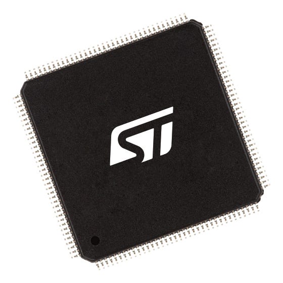 | STM32F407ZET6 | STMicroelectronics | 9,840 | |
| STM32F407ZGT6 | STMicroelectronics | 5,640 | |
| STM32F417VET6 | STMicroelectronics | 3,430 |
No. STM32F407VET6 includes a 10/100 Ethernet MAC and connects to an external PHY through MII or RMII. For a copper Ethernet port, the board also needs the PHY's required supporting circuitry and cable interface. Selecting Ethernet in a configuration tool does not add those physical components. Review the PHY, clock, power and connector arrangement together before expecting traffic at the MCU. ST DS8626, Ethernet interface solutions.
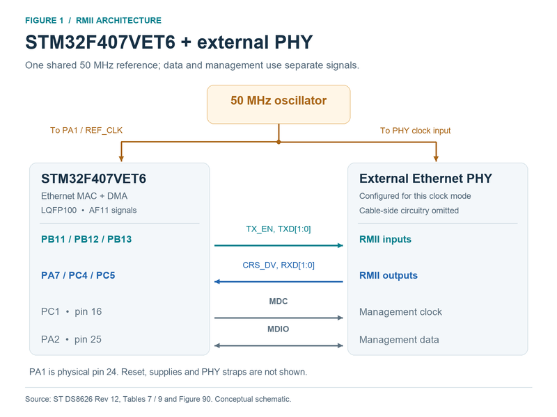
Use PA1 for REF_CLK, PA7 for CRS_DV, PC4/PC5 for RXD0/RXD1, and PB11/PB12/PB13 for TX_EN/TXD0/TXD1. PHY management uses PA2 for MDIO and PC1 for MDC. These Ethernet functions use AF11. Use DS8626's LQFP100 pin column to compare GPIO names with the physical package pins. PG11, PG13 and PG14 from larger-package examples are unavailable here. ST DS8626, pinouts and alternate functions.
A 25 MHz crystal can be part of an appropriate clock arrangement, but PA1 still needs the 50 MHz RMII reference. ST shows a PHY with a PLL producing that reference from a 25 MHz input; the selected PHY must support the arrangement and output mode. Trace the complete path instead of assuming the crystal frequency is what reaches the MCU. The 50 MHz requirement remains at a 10 Mb/s link rate. ST DS8626, Appendix A.3.
The STM32F407VET6 has a 10/100 Ethernet MAC and needs an external PHY. For its 100-pin package, start with the RMII pin map, trace the 50 MHz reference clock, and check the Ethernet supply requirements. Then make sure the DMA can reach its descriptors and packet buffers. A lit link LED is useful, but it does not tell you whether the MCU is moving frames or the network stack is responding.
By Scarlett Zhang
STMicroelectronics puts the Ethernet media access controller, or MAC, inside the STM32F407VET6. The external physical-layer transceiver, or PHY, handles the connection toward the cable. Between them, you can use the media-independent interface, MII, or its reduced-pin counterpart, RMII. This article follows RMII because its wiring exposes several practical checks on the 100-pin package. The hardware arrangement comes from DS8626, Ethernet interface and application diagrams.
A board also needs the PHY's supporting power and clock circuitry, the appropriate cable-side interface, and software that moves received frames into a network stack. Those responsibilities remain even if a development tool can generate most of the initialization code. A configuration file cannot establish that the fitted PHY has the address the driver expects or that a clock reaches the correct pad.
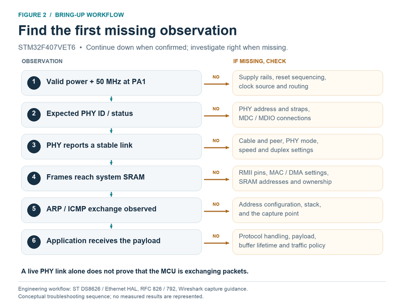
**Figure 1.** A shared 50 MHz source clocks the MCU RMII interface and a PHY configured for this clock mode; MDC and MDIO provide a separate management path. Sources: [DS8626 Appendix A.3 and LQFP100 pin tables](https://www.st.com/resource/en/datasheet/stm32f407ve.pdf#page=190). Conceptual schematic. **Figure 2.** Check the first missing observation before moving to the next layer. A live PHY link alone does not establish that the MAC, DMA, and network stack are exchanging packets. Editorial troubleshooting workflow based on the documented device architecture.A reported PHY link does not establish that frames are reaching the MCU's stack. Check where the exchange stops: the capture point, RMII receive activity, DMA-completed frames, address resolution, or the echo response. Also confirm the test host's network configuration and traffic policy. An IPv4 ARP exchange followed by matching ICMP requests and replies gives more useful evidence than the link indicator alone. This is a diagnostic sequence; the symptom does not identify one universal cause. Protocol references: RFC 826, ARP and RFC 792, ICMP Echo.
No. On STM32F407VET6, the 64 KB CCM is on the core's data path and is not accessible to Ethernet DMA through the bus matrix. Place descriptors and directly accessed packet buffers in suitable system SRAM, then verify their final addresses. Checking a descriptor array is insufficient if its data pointer still targets CCM. SRAM1 spans 0x20000000–0x2001BFFF; SRAM2 spans 0x2001C000–0x2001FFFF. ST DS8626, bus matrix and memory mapping.
Consider STM32F407VGT6 when the application needs more Flash: it provides 1 MB, compared with VET6's 512 KB, in the LQFP100 package class. Confirm the actual application and update-storage requirements first. Then check the selected part, linker layout, bootloader assumptions, electrical suitability and regression results. It is a capacity comparison, not a remedy for incorrect RMII wiring or DMA placement. ST STM32F407VG and DS8626 ordering information.
Start by recording the exact MCU. The E in VET6 selects 512 KB of Flash. A family headline saying “up to 1 MB” describes another capacity option; it does not give this device extra memory. The V selects 100 pins, which matters when an example project routes Ethernet through pins available on a larger package.
Table 1. STM32F407VET6 facts that affect Ethernet bring-up
| Item | Value for this device | Design consequence |
|---|---|---|
| Flash | 512 KB | Budget the bootloader, application, network stack, and any update storage against this capacity. |
| Core clock | Up to 168 MHz, subject to operating conditions | Check voltage scaling and Flash access settings for the chosen clock. |
| Main SRAM | 192 KB total: 112 KB SRAM1, 16 KB SRAM2, 64 KB CCM | Ethernet DMA cannot use all of this as one interchangeable buffer pool. |
| Package | LQFP100; 14 × 14 mm body; 0.5 mm pitch | Verify the 100-pin column and distinguish body dimensions from the lead envelope. |
| Ethernet block | 10/100 MAC with MII/RMII | An external PHY is required. |
| Ethernet operating VDD | 2.7–3.6 V | The MCU's general 1.8 V lower limit does not establish Ethernet operation at that voltage. |
| RMII clock | 50 MHz reference | Trace its source and destination independently of the CPU clock. |
Sources: DS8626, Tables 2, 14, 63 and 93; ordering information; Appendix A.3, and the STM32F407VE product page.
The 10/100 designation describes the Ethernet interface rates. Application throughput also depends on frame handling, memory, protocol overhead, and processing load. For initial bring-up, aim to observe a correctly handled frame. Throughput measurements become useful once that path is repeatable.
On STM32F407VET6, the practical RMII connection uses seven interface signals plus MDC and MDIO for PHY management. All nine signals below use alternate function AF11. The directions are relative to the MCU, and the physical pin numbers apply specifically to LQFP100. They are checked against DS8626, Figure 13 and Tables 7 and 9.
Table 2. RMII and management signals on STM32F407VET6 LQFP100
| Signal | GPIO | Physical pin | MCU direction | AF | Connection or multiplexing check |
|---|---|---|---|---|---|
| ETH_RMII_REF_CLK | PA1 | 24 | Input | AF11 | Route the valid 50 MHz reference to this pin. |
| ETH_MDIO | PA2 | 25 | Bidirectional | AF11 | Shares the pin with functions including USART2_TX. |
| ETH_RMII_CRS_DV | PA7 | 32 | Input | AF11 | Shares the pin with functions including SPI1_MOSI. |
| ETH_RMII_RXD0 | PC4 | 33 | Input | AF11 | Connect to the corresponding PHY receive-data output. |
| ETH_RMII_RXD1 | PC5 | 34 | Input | AF11 | Keep the receive bit order consistent with the PHY. |
| ETH_RMII_TX_EN | PB11 | 48 | Output | AF11 | Also multiplexed with I2C2_SDA, USART3_RX and ULPI_D4. |
| ETH_RMII_TXD0 | PB12 | 51 | Output | AF11 | Also multiplexed with SPI2_NSS, CAN2_RX and ULPI_D5. |
| ETH_RMII_TXD1 | PB13 | 52 | Output | AF11 | Also multiplexed with SPI2_SCK, CAN2_TX and ULPI_D6. |
| ETH_MDC | PC1 | 16 | Output | AF11 | Physical pin 16 is PC1; pin 15 is PC0. |
Source: DS8626, LQFP100 pin assignments and AF11 mapping, pp.44, 50–55 and 64–66. Listed conflicts are examples, not the complete alternate-function inventory.
Begin the schematic review at the MCU symbol, then follow each net to the PHY. A net named RMII_TXD0 should leave PB12 and reach the PHY's corresponding transmit-data input. Check the receive direction separately. Similar-looking signal names on different devices can make it easy to connect two outputs or swap data bits while the drawing still looks tidy.
The package column deserves its own check. PG11, PG13 and PG14 appear in larger-package Ethernet examples, but they are not available on this LQFP100 device. Changing a software pin definition cannot create those physical connections. DS8626 explicitly identifies the absence of Ports F and G on the 100-pin package in its pinout notes. If a borrowed project uses Port G, compare its intended transmit signals with PB11, PB12 and PB13 in Table 2 before adapting it.
Then look for a second peripheral claiming one of these pins. A debug UART assigned to PA2 or an SPI interface assigned to PA7 can undo an otherwise sensible Ethernet configuration. Review the final pin initialization and the order in which other drivers start. The useful question is whether each pin still has its intended function when Ethernet begins operating.
Also separate the nine interface and management signals from the PHY's additional requirements. Reset, address straps, interrupt connections and supply pins depend on the chosen PHY and board. They do not disappear because they are absent from Table 2. Keep those details alongside the PHY documentation instead of copying values from a board with a different transceiver.
The STM32F407VET6 RMII interface needs a 50 MHz reference at PA1. A 25 MHz crystal somewhere on the board is not, by itself, evidence that this input is correct. Follow the clock path through the device that generates the reference and check what actually arrives at the MCU.
ST shows two relevant arrangements in DS8626, Figures 90 and 91. One uses an external 50 MHz oscillator shared by the MCU interface and a PHY configured for that clock input. The other uses a PHY with a PLL that produces the required 50 MHz reference from an appropriate 25 MHz input. These are different clock architectures, so establish which one your board implements.
Table 3. Two ways to supply the RMII reference clock
| Architecture | Clock at the MCU's PA1 | PHY requirement | What to verify on the board |
|---|---|---|---|
| Shared 50 MHz oscillator | 50 MHz from the external source | Accepts the supplied reference in the selected RMII mode | The same source reaches both intended clock inputs; voltage, loading and startup behavior suit both devices. |
| PHY generates the RMII reference | 50 MHz output from the PHY | Supports the required PLL/reference-output mode with the chosen input | The correct output mode is selected, the output is enabled, and the clock reaches PA1 when needed. |
Source: DS8626, Appendix A.3, pp.190–191. Figure 91 specifically shows a 25 MHz PHY input derived directly from the MCU HSE oscillator before the PLL; other PHY input arrangements require that PHY's documentation.
First, what clocks the MCU core and AHB bus? Second, what clock or crystal does the PHY require? Third, what generates the RMII reference received at PA1? Write down each answer separately. The ST application diagrams require HCLK to be greater than 25 MHz. They also show the RMII interface using its 50 MHz reference for both 10 and 100 Mb/s operation, with different internal division. Keep that reference in place when the link negotiates the lower rate.
If the PHY supplies the reference, examine when that output becomes active. Its behavior around reset and configuration matters to the MCU's initialization. If an external oscillator supplies the reference, examine startup and loading at both destinations. In either arrangement, identify one intended driver for each clock net before investigating firmware timeouts.
Measure the reference close to PA1, using probing appropriate for the signal, and compare the waveform with the receiving device's requirements. An oscillator output can look healthy while a routing error, excessive loading, or a poor connection leaves the MCU with a different waveform. Frequency alone also does not establish acceptable logic levels or timing margin.
For example, DS8626 Table 65 gives RMII receive-data setup and hold minima of 2 ns and 1 ns. Those values accompany the Ethernet measurement conditions on p.133, including a 30 pF load, GPIO OSPEEDR setting 10 in binary, and measurements at 0.5 VDD. The CRS_DV requirements and transmit delays have their own entries. Check the PHY's timing on the other side of the connection, then account for clock and data propagation on your board. That calculation tells you what margin the routing needs to preserve. DS8626, Ethernet timing, pp.133–134.
Once the reference is present and the pin assignment is correct, you have a much better basis for investigating PHY communication.
Check the supply and reset conditions before interpreting a failed PHY register read. The MCU, the transceiver, and the clock source each need to be operating correctly for the intended arrangement. A voltage measured at the regulator output is only the start; inspect the rails at the devices and watch what happens during startup.
For the MCU, keep the Ethernet VDD requirement of 2.7–3.6 V in view. The LQFP100 device also uses the internal regulator arrangement described by ST, with external capacitors at VCAP_1 and VCAP_2. DS8626 specifies 2.2 µF and ESR below 2 Ω for these capacitors. These connections stabilize the internal regulator and should follow ST's circuit. Check the PHY's supply connections separately. DS8626, regulator connections and VCAP requirements, pp.31 and 84.
The PHY requires a separate check against its own documentation. Record its supply rails, reset polarity and timing, RMII selection, address straps, and clock configuration. A board can have the right MCU pin map and still leave the PHY in an unintended operating mode. Check whether any pins used for startup configuration are also connected to LEDs or other loads that affect the selected state.
MDC and MDIO form the management path. Use that path to read documented PHY identification or status registers before drawing conclusions from application traffic. Check the transaction's return status as well as the returned value. ST's Ethernet HAL source implements PHY-register reads with an address, a register selection, and a completion timeout; a software call returning is not sufficient evidence that the expected PHY responded.
If the expected response is missing, work through a short sequence: confirm the configured address against the board's straps; observe MDC during an attempted transaction; inspect MDIO at both devices; and verify the PHY's reset and clock conditions. Check its required management-interface pull-up and logic levels as well. Avoid changing the address, reset delay, clock source and pin mapping together. A single change followed by the same observation is easier to interpret.
Once management reads are reliable, compare the PHY's reported operating state with the MAC configuration. Link speed and duplex need to agree across the interface. Keep the PHY-specific interpretation in its driver and documentation; a status bit copied from another transceiver may mean something different.
At this point, record what you have established: device power, a usable reference clock, and repeatable communication with the intended PHY. That gives the next stage a concrete starting point. It still leaves the movement of Ethernet frames through MCU memory to be checked.
Ethernet DMA on STM32F407VET6 can access the system SRAM banks, but it cannot access the 64 KB CCM through the same path. The CPU's ability to read a buffer therefore does not establish DMA access. ST's bus matrix and memory map make this distinction explicit. DS8626, Figure 6 and Figure 18.
Direct memory access, or DMA, moves frame data between memory and the Ethernet peripheral. Descriptors tell it where the buffers are and provide transfer state. Both the descriptors and every buffer that DMA accesses directly need valid placement. Checking only the array that stores descriptors leaves half the problem unresolved.
Table 4. Internal RAM placement for Ethernet descriptors and buffers
| Memory region | Capacity and address range | CPU access | Ethernet DMA access | Practical use |
|---|---|---|---|---|
| SRAM1 | 112 KB; 0x20000000–0x2001BFFF | Yes | Yes, through the bus matrix | Candidate space for descriptors and frame buffers, subject to allocation and driver requirements. |
| SRAM2 | 16 KB; 0x2001C000–0x2001FFFF | Yes | Yes, through the bus matrix | Another accessible region; account for its size and other users. |
| CCM data RAM | 64 KB; 0x10000000–0x1000FFFF | Yes, through the core data path | No | CPU-only data whose placement does not expose it to Ethernet DMA. |
Source: DS8626, SRAM organization, bus matrix and memory map, pp.22–23 and 73. The separate backup SRAM is not included as a default Ethernet buffer pool.
Open the linker's map file and locate the descriptor arrays and packet-buffer storage. Then inspect their actual addresses during execution. A declaration placed in a named section helps only if the linker maps that section where you intended. A memory allocation made at runtime deserves the same check.
Pay attention to the whole data path. A descriptor may sit in SRAM1 while pointing to data allocated elsewhere. If a driver transmits directly from an application's buffer, that buffer's address matters too. Moving an unrelated working array out of CCM will not repair the address supplied to DMA.
Table 4 also explains why a simple total-RAM calculation can mislead you. The two system SRAM banks provide 128 KB together, and that space may already contain stacks, heap allocations and other peripheral buffers. Your network allocation must fit alongside those users. Keep a memory budget for the actual linked application, then examine how much remains under the intended workload.
Accessible memory is necessary, but the driver must also hand buffers over and reclaim them correctly. In ST's Ethernet HAL implementation, receive processing checks descriptor ownership; replenishing descriptors requires available buffers. Review those paths in the exact driver version your project uses.
For transmit, keep the data valid until the driver has finished with it. A pointer into a temporary object is a reason to inspect lifetime, even when its address is inside accessible SRAM. For receive, track whether the application releases data promptly enough for buffers to be reused. These checks concern how your program uses the memory, so changing the peripheral clock will not resolve them.
Prefer a small diagnostic record over repeated printing inside every receive callback. Track allocation failures, descriptors returned, and frames delivered to the stack. Add timestamps or sequence numbers when they help connect an event to a test packet. The resulting record should show where progress stops without introducing so much logging that it changes the workload you are trying to observe.
After the PHY responds and the link is established, trace one simple exchange through the MCU. Keep the observations from the cable, DMA and stack separate. When a request produces no reply, those observations will help you choose the next measurement.
Use a controlled network arrangement with a known test peer. Record the board's MAC address, IP configuration, link state, and software build. For an initial IPv4 test, you can use deliberately assigned addresses on the same subnet where the test network permits it. This removes reliance on a DHCP server while you examine the frame path. Keep those test settings distinguishable from the eventual deployment configuration.
Start the capture on the interface that carries the test traffic. If the capturing computer is the actual peer, inspect traffic to and from that connection. A computer plugged into an unrelated port of a switch will not necessarily see the board's unicast exchanges. Wireshark documents capture arrangements such as a suitable mirror port or network tap, with limitations that depend on the setup. Wireshark, Ethernet capture setup.
This matters when interpreting absence. “Nothing appeared in the capture” becomes useful only after you know that the capture point should have seen the packet. Compare that observation with what the transmitting application and the MCU's receive path report before concluding that a physical connection is broken.
For IPv4 over Ethernet, Address Resolution Protocol, or ARP, maps a local protocol address to an Ethernet address. When the peer needs that mapping and lacks a usable entry, an ARP request and reply give you an observable exchange to inspect. A cached mapping can remove the need for a new request, so do not assume every ping begins with visible ARP traffic. RFC 826, address resolution and packet generation.
If a request for the board's address is visible at the peer, compare it with the MCU's receive observations. Does a completed frame reach memory? Is it passed to the stack? Does the stack recognize the target address and attempt a reply? Those observations split a receive-path problem from an address-configuration or response-path problem.
If a reply is prepared in software but never appears at the peer, inspect transmit buffer addresses, transfer status, and activity at the RMII transmit signals. If the peer receives the expected reply, you have evidence for a specific exchange through both directions. Keep the capture and the corresponding MCU observations together; each tells you something different about where the frame traveled.
With address resolution working, examine ICMP echo requests and replies. ICMP defines the echo identifiers, sequence numbers, and returned data that let you match a reply to a request. Use those fields to confirm that the response belongs to your test instead of treating any traffic as success. RFC 792, Echo or Echo Reply Message.
A missing reply can still involve the test host's policy, address settings, the MCU's protocol handling, or the transmit path. Narrow it by asking where the matching request was last observed. If it reached the MCU's stack, repeating the same physical-pin review gives you less information than examining the next software decision.
Once ping is repeatable, exercise the protocol your product actually uses. Send a recognizable payload and verify its content at the receiving application. Repeat the exchange, reconnect the cable, and restart the board as appropriate for your use case. These are proposed validation steps, not reported test results. A successful short exchange establishes a useful baseline; it does not characterize throughput, long-duration behavior, or every recovery path.
ST's ES0182 Rev 19, dated July 2026, states that automatic Ethernet pause-frame transmission is not supported as described in §2.16.12. Its software workarounds involve monitoring receive-buffer availability. Account for this limitation when examining behavior under incoming traffic; do not assume the hardware will automatically prevent receive-buffer exhaustion. ES0182, §2.16.12, p.36.
Record the actual silicon revision and review the errata that apply to the functions your application uses. For this bring-up exercise, a useful next test is to compare quiet traffic with controlled bursts while watching buffer availability and dropped-frame indicators. The question is whether your application can keep returning resources as traffic arrives. That is a more focused investigation than assuming a stable link implies unlimited receive capacity.
Keep STM32F407VET6 as the reference point while evaluating nearby parts. It provides 512 KB of Flash in LQFP100; a different memory capacity or package is useful when it addresses a measured design constraint. The four STMicroelectronics parts below offer distinct comparisons without establishing a blanket replacement claim.
Table 5. Four related MCUs and the design changes they imply
| Related MPN | Flash | Package | Reason to compare it | What still needs checking |
|---|---|---|---|---|
| STM32F407VGT6 | 1 MB | LQFP100 | More Flash while staying in the 100-pin package class | Pin and electrical suitability, linker settings, bootloader and update layout, and regression testing. |
| STM32F407ZET6 | 512 KB | LQFP144 | More physical pin options while retaining the same Flash capacity | PCB footprint, power connections, signal reassignment and peripheral conflicts. |
| STM32F407ZGT6 | 1 MB | LQFP144 | More Flash and more pin options together | Both board changes and software memory layout; a new package requires layout work. |
| STM32F417VET6 | 512 KB | LQFP100 | Hardware cryptographic capability in a similar capacity and package class | Detailed pin/electrical compatibility, software support, and the complete security design. |
Sources: ST's exact-part listings and product summaries for STM32F407VG, STM32F407ZE, STM32F407ZG, and STM32F417VE; F407 capacity and package coding are also covered by DS8626, Table 2 and ordering information.
STM32F407VGT6 is a relevant comparison when the linked image and planned updates exceed the available Flash budget. Before changing parts, identify what consumes the space and what the update scheme requires. More Flash expands that budget; it does not supply a missing reference clock or make CCM accessible to Ethernet DMA. Review the selected part and memory settings in the build as carefully as the physical component.
STM32F407ZET6 addresses a different constraint. A design may have enough program storage but too many peripherals competing for the pins available in LQFP100. Moving to LQFP144 gives the schematic more pin options, at the cost of a different footprint and routing work. Check whether the additional assignments actually solve the conflict before committing to the board change.
STM32F407ZGT6 combines the two changes. If both Flash usage and pin assignment are tight, review how the larger capacity and package would affect the design together. Include board size, the memory map, and the validation work in that decision.
STM32F417VET6 adds a reason to compare hardware cryptographic functions. Those functions are a component of a security implementation; protocol software, key handling and application requirements still need their own design work. The comparison here verifies the listed product characteristics, not a complete pin-by-pin replacement or a security qualification.
Whichever part you consider, write down the constraint that prompted the comparison and the evidence that the candidate addresses it. That keeps component selection connected to the board you are building.
For STM32F407VET6, useful progress begins with the exact 100-pin wiring and a valid 50 MHz reference at PA1. Add repeatable PHY communication, DMA-accessible memory, and an observed frame exchange. Each result gives the next check a firmer basis.
When traffic stops, return to the last point where you could observe it and inspect the next part of the path. Keep the schematic revision, build, addresses and capture together so that a successful run can be repeated. Once that baseline holds, move on to application traffic, recovery and load testing. Those later tests are what turn a first packet into a dependable network connection.