
Veca Huang




| Picture | Part Number | Manufacturer | Stock | Action |
|---|---|---|---|---|
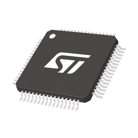 | STM32F103RCT6 | STMicroelectronics | 7,560 | |
| STM32F103RDT6 | STMicroelectronics | 6,410 |
For the stated normal-mode examples with SJW = 1 tq, 500 kbit/s uses physical prescaler 4, BS1 = 13 and BS2 = 4, giving CAN_BTR = 0x003C0003 and a 77.8% sample point. The 1 Mbit/s example uses prescaler 3, BS1 = 8 and BS2 = 3, giving 0x00270002 and a 75% sample point. Recalculate when PCLK1 or the physical-network timing requirements change.
The device has 14 banks. One bank in 32-bit mask mode stores one identifier/mask pair, while 16-bit mask mode stores two pairs. In list mode the same bank stores two 32-bit identifiers or four 16-bit identifiers. Filter capacity is separate from the two receive FIFOs, each of which holds three complete messages.
Bus-Off occurs when TEC exceeds 255. With ABOM = 1, bxCAN monitors for 128 occurrences of 11 consecutive recessive bits before recovery. At 500 kbit/s the ideal continuously idle lower-bound interval is 2.816 ms; active or faulty bus conditions can extend it. ABOM is not a fixed millisecond timer or a correction for the fault that caused Bus-Off.
By Veca Huang | YG GROUP
STM32F103RCT6 CAN bring-up requires a verified APB1 clock, minus-one encoding of CAN_BTR fields, and filters configured for the intended identifier format. At PCLK1 = 36 MHz, 500 kbit/s with 18 time quanta uses BTR = 0x003C0003, while a 12-time-quanta 1 Mbit/s example uses 0x00270002. Bus-Off recovery depends on recessive bus sequences; this high-density device also shares an exclusive 512-byte buffer between USB and CAN.
STM32F103RCT6 is a high-density STM32F103 with 256 KB Flash, 48 KB system SRAM and a 72 MHz Cortex-M3 core. Its bxCAN controller supports CAN 2.0A and 2.0B active operation up to 1 Mbit/s, three transmit mailboxes, two receive FIFOs with three complete messages each, and 14 filter banks. Do not import the 28-bank, dual-CAN arrangement of STM32 connectivity-line devices into this part.
The APB1 peripheral clock is the timing input for bxCAN. A 72 MHz core does not mean that CAN is clocked at 72 MHz: the device’s maximum APB1 frequency is 36 MHz. Confirm the actual clock tree before programming CAN_BTR, and confirm the oscillator tolerance and physical network’s propagation budget before treating a nominal baud-rate calculation as a complete timing design.
High-density memory does not remove the USB/CAN restriction. RM0008 explicitly states that USB and CAN share a dedicated 512-byte SRAM exclusively and cannot operate concurrently on this device. Moving CAN to remapped pins only changes signal routing. If simultaneous CAN and USB traffic is required, resolve the peripheral-resource architecture before debugging the board.
No. On STM32F103RCT6, USB and CAN share a dedicated 512-byte SRAM exclusively. Pin remapping does not create separate peripheral buffers. The larger STM32F103RDT6 system SRAM also does not remove this limitation. Use an architecture with separate resources if simultaneous USB and CAN operation is required.
Use physical values first: one nominal bit contains SYNC_SEG = 1 tq, BS1 time quanta before the sample point, and BS2 time quanta after it. For prescaler P, the time quantum is P / PCLK1. The bit rate is PCLK1 / [P × (1 + BS1 + BS2)], and the sample point is (1 + BS1) / (1 + BS1 + BS2).
CAN_BTR stores P − 1, BS1 − 1, BS2 − 1 and SJW − 1. Mixing physical segment lengths with encoded register fields is a common source of a plausible-looking but incorrect hexadecimal value.
Table 1. Calculated bxCAN bit-timing examples | Source: manufacturer documents in References; assumptions and operating conditions are stated in the table or adjacent text. Compiled / calculated by: YG GROUP.
| Nominal bit rate | Physical P / BS1 / BS2 / SJW | Time quanta per bit | Sample point | CAN_BTR, normal mode |
|---|---|---|---|---|
| 500 kbit/s | 4 / 13 / 4 / 1 | 18 | 14 / 18 = 77.8% | 0x003C0003 |
| 1 Mbit/s | 3 / 8 / 3 / 1 | 12 | 9 / 12 = 75.0% | 0x00270002 |
Both examples assume PCLK1 = 36 MHz and SILM = LBKM = 0. The 500 kbit/s check is 36 MHz / (4 × 18) = 500 kbit/s. Its encoded fields are BRP = 3, TS1 = 12, TS2 = 3 and SJW = 0. The 1 Mbit/s example similarly uses BRP = 2, TS1 = 7, TS2 = 2 and SJW = 0.
/* Encode physical values already validated for the actual network. */
uint32_t btr = ((sjw - 1U) << 24)
             | ((bs2 - 1U) << 20)
             | ((bs1 - 1U) << 16)
             |  (prescaler - 1U);
/* Program CAN_BTR only after CAN initialization mode is acknowledged. */
The formula fragment does not initialize GPIO, clocks or the peripheral, and it assumes valid ranges and SJW ≤ BS2. It is not a complete driver. The sample points above are examples; cable delay, oscillator tolerance and transceiver timing can require a different valid solution at the same bit rate.

Figure 1. Calculated nominal timing at PCLK1 = 36 MHz, SJW = 1 tq and normal mode: 500 kbit/s uses 18 tq, prescaler 4, 77.8% sampling and BTR 0x003C0003; 1 Mbit/s uses 12 tq, prescaler 3, 75% sampling and BTR 0x00270002. The state flow shows Error Passive when TEC or REC exceeds 127, Bus-Off when TEC exceeds 255, and automatic recovery after 128 occurrences of 11 consecutive recessive bits with ABOM = 1. Source: RM0008 Rev 21 §§24.7.6–24.7.7 and CAN_MCR / CAN_BTR.
Each RCT6 bank contains two 32-bit filter registers. In 32-bit mask mode, they form one identifier/mask pair. In 16-bit mask mode, the same storage forms two pairs. List mode instead stores two 32-bit identifiers or four 16-bit identifiers. A bank is therefore not always “two masks” or “four identifiers”; its scale and mode determine what those registers mean.
For one exact standard data-frame ID, 0x123, a 32-bit mask example is:
uint32_t id_word   = 0x123U << 21;          /* 0x24600000 */
uint32_t mask_word = (0x7FFU << 21)
                   | (1U << 2) | (1U << 1); /* 0xFFE00006 */
The mask checks all 11 standard identifier bits, IDE and RTR. The identifier word leaves IDE = 0 and RTR = 0, so the filter admits the selected standard data frame and rejects extended or remote frames that would otherwise share some identifier bits. Acceptance follows (received_word & mask_word) == (id_word & mask_word). Software API fields may split these words into high and low halfwords; preserve the bit positions when using that API.
Enter filter initialization mode, set the bank’s scale and mask/list mode, program its values and FIFO assignment, activate the bank, and leave filter initialization before expecting normal reception. Read the chosen FIFO, then release its entry. Filter matching does not consume an unlimited software queue: each hardware FIFO still holds only three messages, so firmware service and overrun policy matter under load.
Error Active and Error Passive describe the controller’s error confinement state. Error Passive is entered when TEC or REC exceeds 127; Bus-Off occurs when TEC exceeds 255. In Bus-Off, bxCAN cannot transmit or receive. Record CAN_ESR, transmit results and receive status when diagnosing faults rather than inferring the state from one failed mailbox request.
With CAN_MCR.ABOM = 1, automatic recovery waits for 128 occurrences of 11 consecutive recessive bits on CAN_RX. The recovery is bus-condition dependent. At 500 kbit/s, 128 × 11 × 2 µs gives a continuously idle lower bound of 2.816 ms; it is not a fixed recovery timer for an active bus. With ABOM = 0, software must request and leave initialization before the monitored recovery sequence. While the controller remains in initialization, CAN_RX is not monitored for that recovery sequence.
Automatic recovery also does not repair wrong baud rate, missing common ground, a transceiver held in standby or a damaged bus. Avoid repeatedly returning application traffic to a persistent fault without diagnostics. Likewise, do not claim that any missing ACK inevitably drives TEC to Bus-Off; CAN error-counter rules include exceptions. Observe the actual flags and counters, and validate that healthy communication returns after the fault is removed.
The MCU’s CAN pins are logic signals, not a differential cable interface. In the default LQFP64 mapping, PA12 / CAN_TX is pin 45 and PA11 / CAN_RX is pin 44. Connect TX to the external transceiver’s TXD input and its RXD output to RX. Select a transceiver with a compatible logic interface, supply and common-mode range; none of those properties is supplied by bxCAN itself.

Figure 2. Illustrative two-node network using default LQFP64 PA12 / CAN_TX pin 45 and PA11 / CAN_RX pin 44. Each physical end has 60 Ω + 60 Ω in series across CANH and CANL; the midpoint capacitor returns to ground. Capacitor value, transceiver supply and protection details depend on the chosen physical-layer design. No fixed midpoint voltage or measured EMC improvement is asserted. Sources: DS5792 Rev 13 pin table and RM0008 Rev 21 Figure 222 for controller/transceiver topology; split termination is a design illustration. Diagram: YG GROUP.
The split termination example uses two 60 Ω resistors in series across CANH and CANL at each physical end. Their midpoint connects through a capacitor to ground. The 60 Ω + 60 Ω path provides 120 Ω differential termination at one end; the midpoint capacitor is not a series element in the CANH-to-CANL path. Choose the capacitor, grounding and protection details using the selected transceiver’s physical-layer guidance and the application’s tests.
A midpoint is not guaranteed to remain at 2.5 V across different transceiver supplies and common-mode conditions. This illustrative circuit also does not establish a measured EMI improvement, a permissible universal cable length, or automotive qualification. Use short node stubs and measure assembled-bus differential edges and communication behavior at the intended load and temperature.
First verify the peripheral clock and timing fields, then use an appropriate controller test mode to check software transmission, filters and FIFO service. A loopback result cannot validate external wiring or termination. Follow with a physical bus containing another correctly configured node, verify normal ACK behavior, and capture error status during controlled fault and recovery testing.
Table 2. Same-family memory and CAN comparison | Source: manufacturer documents in References; assumptions and operating conditions are stated in the table or adjacent text. Compiled / calculated by: YG GROUP.
| Exact model | Memory specified in DS5792 | CAN boundary relevant to this article |
|---|---|---|
| STM32F103RCT6 | 256 KB Flash, 48 KB SRAM; LQFP64 | One bxCAN, 14 banks; exclusive shared USB/CAN buffer |
| STM32F103RDT6 | 384 KB Flash, 64 KB SRAM; LQFP64 | Same CAN resource boundary; added system memory does not enable USB/CAN concurrency |
The RD part is a real same-family capacity candidate, not an unconditional substitution. Check the memory map, firmware image and board configuration before selecting it. For both parts, retain an explicit record of PCLK1, timing fields, filter format, FIFO service policy, transceiver state and recovery behavior. Those concrete observations distinguish a register-encoding fault from a resource conflict or a physical-layer problem. No completed bench or EMC result is claimed here.