
Ying Lin




| Picture | Part Number | Manufacturer | Stock | Action |
|---|---|---|---|---|
 | RTL8201F-VB-CG | Realtek | 7,120 | |
| RTL8201FN-VB-CG | Realtek | 3,170 | |
 | LAN8720A-CP-TR | Microchip | 8,780 | |
 | DP83848IVV/NOPB | Texas Instruments | 4,220 |
It is a single-port 10/100 Mbps Ethernet PHY with MII and RMII interfaces, supplied in a 32-pin QFN package. The host still needs a compatible Ethernet MAC, frame handling, and network software. Realtek's Rev.1.4 datasheet specifies a recommended ambient range of 0°C to 70°C for the covered device. Do not infer an industrial temperature grade from an embedded application or substitute the pin map of the 48-pin FL or FN family members.
Yes, the documented RMII mode allows the TXC pin to serve as the 50 MHz reference output or input. The CLK_CTL strap and page-7 register-16 setting must agree with the circuit's clock owner. If the PHY output is required, Realtek states that link-down power saving must be disabled for that use. Test clock continuity with the Ethernet cable removed, because the MAC's need for a reference does not necessarily disappear when the copper link goes down.
For the RTL8201F-VB-CG in the adopted Rev.1.4 document, an external 25 MHz or 50 MHz oscillator enters CKXTAL2, pin 32, while CKXTAL1, pin 31, is grounded. A crystal uses a different connection. Read the clock-interface section together with the RMII mode-register note and the chosen reference direction. A generic PHY diagram or another manufacturer's oscillator convention is not a safe substitute for this device's pin-level clock circuit.
By Ying Lin
The RTL8201F-VB-CG is a Realtek 10/100 Mbps Ethernet PHY with MII and RMII interfaces in a 32-pin QFN package. In an RMII design, its reference-clock direction, reset sequence, and power-saving settings need to agree with the connected MAC. If the PHY supplies the MAC's 50 MHz clock, clock continuity becomes a system requirement—even when the Ethernet cable is unplugged. That is the most useful starting point for this device, because its link-down power-saving mode has a specific restriction when the RMII reference output is needed. [1, §§6.3, 7.10, 11]
A networked printer or embedded controller can have a perfectly plausible Ethernet schematic and still fail during first boot or cable recovery. The link LED only describes one part of the path. This guide follows the PHY from its power and strap settings to observable MAC traffic, with particular attention to details that are easy to inherit incorrectly from another Ethernet design.
This article uses RTL8201F-VB-CG, the exact ordering code covered by Realtek's Rev.1.4 datasheet dated 30 November 2011. The F, FL, and FN devices appear together in that document, but their packages and some pin functions differ. The F device is the 32-pin QFN option; the FL is a 48-pin LQFP and the FN a 48-pin QFN. A shared register discussion does not make their pin numbers interchangeable. [1, Tables 59–60]
For the F package, the compact footprint is useful when the processor already provides an Ethernet MAC and the product needs a single copper port. The PHY handles physical-layer transmission and reception. The MAC, frame buffers, DMA behavior, and network software still belong to the host design. A management-register response proves that the PHY is accessible; it does not prove that the processor is sending Ethernet frames.
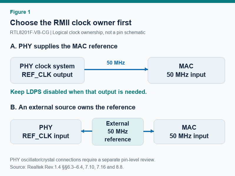
**Figure 1.** Choose the reference-clock owner before setting the strap and power policy. A required PHY-generated output needs the documented LDPS restriction. The diagram shows logical ownership only; oscillator, crystal, and pin-level connections must follow the selected circuit. Based on Realtek Rev.1.4 §§6.3–6.4, 7.10, and 7.16. [1] **Figure 2.** Investigate the earliest missing observation. Management access points toward power, reset, address, and MDC/MDIO; later failures shift attention toward media, RMII timing, and clock continuity. This is an editorial diagnostic sequence derived from the documented architecture, not measured test data. [1]The documented active-low hardware-reset interval is at least 10 ms. The power-on/reset sequence also includes a 150 ms interval before management-register access at the indicated point, with a stable clock and the required supply/reset relationship. These timings perform different jobs; the shorter reset-release timing is not a replacement for register readiness. Software reset only resets part of the register state, so its recovery path should explicitly restore the configuration the board requires.
The copper PHY can form a link while the host-side data path remains misconfigured. First establish stable MDIO identity reads, then inspect link and negotiation status, then observe MAC transmit and receive activity. RMII mode, reference direction, clock continuity, and setup/hold timing remain separate checks. The basic status register also latches link loss, so a second read is needed when interpreting the current state after a recovered link. Host DMA and network software require their own evidence.
No direct replacement qualification is claimed. RTL8201FL-VB-CG and RTL8201FN-VB-CG are related family members with different 48-pin packages and variant details. LAN8720A-CP-TR is a Microchip 24-pin RMII PHY with its own commercial ordering conditions. DP83848IVV/NOPB is a TI 48-pin MII/RMII PHY with an industrial temperature range. Each requires a review of footprint, pin functions, supplies, clocking, straps, software, and the product's operating conditions before use on an existing board.
The documented recommended operating conditions specify a 3.3 V supply range of 2.97–3.63 V and an operating ambient range of 0°C to 70°C. Keep that commercial-temperature boundary visible when discussing applications. A device can be useful in an embedded product without being the right choice for every outdoor cabinet or industrial temperature requirement. [1, Table 47]
Table 1. Device facts that shape the first board review
| Item | RTL8201F-VB-CG evidence | Design meaning |
|---|---|---|
| Function | Single-port 10/100 Mbps Ethernet PHY | Requires a compatible external MAC and the copper-interface components |
| MAC interfaces | MII and RMII | Strap selection and host configuration must agree |
| Package | 32-pin QFN | Use the F pin map, not the FL or FN package drawing |
| Recommended supply | 3.3 V nominal; 2.97–3.63 V range | Check the PHY supply at the device during startup and traffic |
| Recommended ambient | 0°C to 70°C | Do not infer an industrial temperature grade from the application name |
| Internal core supply | Embedded regulators generate 1.1 V | Their outputs serve the PHY; they are not auxiliary board supplies |
| RMII reference | 50 MHz input or output, according to configuration | Assign one clock owner and account for power-state behavior |
Source: Realtek Rev.1.4 §§1–2, 6.3, 8.8, 9.1.2, and 11. Values are datasheet specifications, not measurements from a YG GROUP board. [1]
Before comparing alternative PHYs, establish the host's actual interface requirements. Some MACs accept an external RMII reference; others can supply a reference under specific clock-tree conditions. That is a property of the exact host and its selected mode. A familiar microcontroller family name is not enough to decide the connection.
RMII reduces the data interface width, but it does not make the clock optional. Both sides need the intended reference relationship. On the RTL8201F-VB-CG, the TXC pin becomes the synchronous 50 MHz RMII reference-clock input or output. Its direction is selected through the CLK_CTL strap and the RMII mode register. The documented default direction is output when the strap is left at its internal low state. [1, §§6.1, 6.3, 7.16]
For the 32-pin F package, TXC is pin 15 and RXD3/CLK_CTL is pin 12. These names matter because a generic drawing may call every clock connection “REF_CLK” while hiding which device is driving it. Mark the driver and receiver explicitly on the schematic. Two outputs tied together are not a redundant clock arrangement; two inputs connected together do not create a clock source.
When the PHY supplies the MAC reference, the attraction is a clear clock relationship with fewer independent sources to coordinate. The cost is that the MAC now depends on the PHY's clock behavior. Realtek's power-saving register description states that link-down power saving must be disabled if the REF_CLK output is required in RMII output mode. The relevant enable is register 24 bit 15. [1, §7.10]
That changes how I would test a printer-controller board. I would not stop after a successful transfer with the cable connected. I would remove the cable while observing the reference at the MAC input, then reconnect it and check recovery. The point is to expose a clock dependency during a normal user action, not to invent a rare failure scenario. This test recommendation follows directly from the documented interaction between link-down power saving and the reference output.
Disabling LDPS for a required clock output is a functional decision, not merely a power-consumption preference. Record it with the clock-tree configuration so that a later power-optimization change does not quietly undo it. An Ethernet driver and a power-management module can each look correct in isolation while making contradictory assumptions about that one signal.
If an external source owns the RMII reference, configure the PHY as an input and confirm that the MAC sees the required clock as well. The PHY's own oscillator/crystal connections still require a separate review. A logical diagram showing a shared 50 MHz reference is not a complete pin-level clock circuit for this part.
The distinction is especially important here because Realtek's external oscillator connection is easy to reverse by habit. In Rev.1.4, an external 25 MHz or 50 MHz oscillator drives CKXTAL2, while CKXTAL1 is grounded. For the 32-pin package these are pins 32 and 31 respectively. A crystal uses the crystal connection instead. Do not copy the external-clock pin convention from another manufacturer's PHY. [1, §6.4]
The same datasheet includes a specific page-7 register-16 recommendation for an external clock entering CKXTAL2. Read that note together with the selected reference direction and the entire clock circuit. Treating its hexadecimal value as a universal RMII initialization recipe would erase the conditions under which Realtek gives it. [1, Table 26]
Several pins carry a configuration role around reset and a different signal role during operation. That makes the external loading part of the boot configuration. A resistor, LED network, or host pin that looks harmless after startup can change the logic level the PHY samples when it initializes.
The RMII-select strap is on RXDV, pin 8 in the F package. The documented external 4.7 kΩ pull-up selects RMII; the default is MII. The CLK_CTL strap selects reference input when high and output when low. These are separate decisions: selecting RMII does not by itself establish the correct direction of its clock. [1, §§6.1, 6.7]
Table 2. F-package signals that deserve explicit schematic labels
| Signal and pin | Relevant behavior | Review action |
|---|---|---|
| RXDV / RMII, pin 8 | Strap selects RMII when pulled high as documented | Confirm the reset-time level and the host's selected interface |
| RXD3 / CLK_CTL, pin 12 | High selects REF_CLK input; low selects output | Name the actual clock driver on the schematic |
| TXC, pin 15 | RMII 50 MHz reference input or output | Check direction and waveform at the receiving pin |
| CKXTAL1 / CKXTAL2, pins 31 / 32 | Crystal circuit; external oscillator enters CKXTAL2 with CKXTAL1 grounded | Follow this device's oscillator connection convention |
| LED0 / PHYAD0 and LED1 / PHYAD1, pins 24 / 25 | Sampled address bits share pins with LED functions | Account for LED loading and use the documented resistor arrangements |
| PHYRSTB, pin 21 | Active-low hardware reset | Confirm actual low duration, release timing, and subsequent access delay |
| RSET, pin 1 | 2.49 kΩ, 1% reference resistor to ground | Keep the bias circuit quiet and use the specified tolerance |
Source: Realtek Rev.1.4 §§5.1 and 6.1–6.9. Pin numbers apply only to RTL8201F-VB-CG's 32-pin package. [1]
The two PHY address straps give addresses in the range selected by those bits, rather than an arbitrary address that software can assume from an unrelated evaluation board. The datasheet cautions against directly tying the address/LED pins to power or ground; use its resistor arrangements. A useful first software diagnostic is to report which address returns the expected identifier, then compare that address with the circuit's intended state. [1, §8.4.1]
Wake-on-LAN introduces another shared-pin decision. On this variant, the RXD1 strap participates in choosing the LED or wake function, and the wake configuration has address restrictions described in the datasheet. If wake support is required, include it in the initial pin review rather than bolting it onto an already-frozen LED circuit. The interrupt function on the F package also has an RMII-specific restriction. [1, §§6.1, 8.11, Table 60]
These interactions are why I would keep a short reset-time pin-state table beside the schematic. It should show the PHY's intended level, the external resistor, and what the connected host pin does during reset. It records the reset-time loading that a normal run-state net label cannot show.
The internal regulators simplify the supply arrangement, but their output pins still need the specified capacitors. Realtek describes a 0.1 µF X5R low-ESR ceramic capacitor as part of the regulator's compensation. The 1.1 V outputs are intended only for the PHY. The F and FL variants cannot disable their internal regulators, so driving those nodes from an external core supply can create a conflict. [1, §8.8]
The internal regulators reduce external supply circuitry, but their output nodes still need attention. “Internal regulator” does not mean “ignore the output node,” and it does not turn the PHY into a convenient source for a neighboring circuit. Review its local capacitors and return paths as part of the PHY supply rather than as generic bulk decoupling.
The PHYRSTB pin requires a low interval of at least 10 ms for the documented hardware reset. The power-on/reset sequence also specifies a 150 ms interval before register access at the indicated point in the sequence. Its table includes the relationship between supply stability and reset release. Use the complete sequence, including a stable clock, rather than selecting the smallest delay that happened to work once. [1, §§6.9, 8.7, 9.1.3]
A board with a fast processor boot can reach its Ethernet initialization routine before the PHY is ready. If the driver interprets the first failed management read as a permanently missing device, the symptom may look intermittent even though the timing is deterministic. Put the PHY-ready interval in a deliberate initialization state and make failed identity reads visible in the boot log.
Table 3. Startup values and what they do—and do not—prove
| Requirement or observation | Documented value or meaning | Interpretation |
|---|---|---|
| Hardware reset low interval | At least 10 ms | A shorter pulse is outside the stated reset requirement |
| Register-access readiness | 150 ms in the documented power-on/reset sequence | Follow the sequence and its stable-clock condition |
| Reset release after 3.3 V stability | At least 80 µs in Table 48 | This timing does not replace the longer register-readiness requirement |
| Management clock | MDC up to 2.5 MHz | Configure the host divider for its actual source clock |
| Initial management preamble | Thirty-two consecutive ones after reset | Do not assume a shortened frame is accepted at first access |
| PHY identifier read | Registers 2 and 3 identify the device | Management access is established; MAC traffic remains unproven |
| Software reset | Partially resets registers and reinitializes state | Do not assume it reproduces every hardware-reset condition |
Source: Realtek Rev.1.4 §§6.2, 7.3–7.4, 8.1.2, 8.7, and 9.1.3. Timings refer to the documented conditions, not a measured board boot time. [1]
Software reset deserves its own handling. It resets only part of the register state, unlike the documented hardware-reset behavior. That difference matters when a driver recovery path assumes that straps, extended registers, and power-saving settings have all returned to one known baseline. Define which settings the recovery path restores, and verify them after the reset operation it actually uses. [1, §8.7]
Once the reset sequence is repeatable, read the identifier before making several configuration changes at once. A clean progression—identity, mode, clock direction, then link and traffic—makes later observations easier to interpret. If the first read is already unreliable, adjusting receive timing offsets only adds another variable.
The management path is a distinct interface from RMII data transfer. MDC is supplied by the host and MDIO is bidirectional. A working MDIO transaction can therefore coexist with a broken RMII clock, incorrect data-pin assignment, or a MAC that has not started its transmit engine. Use that separation to establish management access before diagnosing frame transfer. [1, §§6.2–6.3]
Start with stable identifier reads at the expected address. Then inspect the interface and power configuration relevant to the board. The device uses register 31 for page selection, so an extended-register operation must make its page context explicit. Restore the intended page before ordinary accesses. An apparently nonsensical “standard register” value can be a page-selection mistake rather than an analog fault. [1, §§7.13–7.21]
The basic status register's link bit latches a loss of link. A read can therefore report the captured loss even after the physical connection has recovered. Read it again when the task is to observe the present state, while preserving the first result if historical loss is useful to the diagnostic log. Otherwise, software can report a disconnected cable after the link is already back. [1, §7.2]
Auto-negotiation adds another distinction. With auto-negotiation enabled, the forced speed and duplex bits do not simply override the negotiation result. Parallel detection can establish a link with a partner that does not negotiate, but it does not provide the same information as a completed negotiation; the documented duplex outcome must be handled accordingly. A live link is not permission to assume both ends agreed on full duplex. [1, §§7.1, 8.3]
For the first traffic test, record the partner's configuration as well as the local registers. That makes a duplex mismatch or unexpected speed visible in the evidence instead of turning it into a vague “Ethernet is slow” problem. Use a known cable and partner for this initial step, then widen the test conditions once the local configuration is understood.
At 50 MHz, one reference-clock period is 20 ns. That number describes the cycle, not the available setup margin. The PHY's transmit-input specification includes a 4 ns minimum setup time and a 2 ns minimum hold time. Clock routing, host output timing, and loading determine where the data actually lands relative to those limits. [1, Table 53]
The datasheet also provides receive timing information, but its table must be read by column. The 2 ns entry for receive output delay is in the minimum column; it is not a stated maximum delay that can be used to close the entire MAC receive budget. If the host-side analysis needs a bound that the adopted table does not supply, do not invent it from the one visible number. [1, Table 53]
Table 4. RMII timing observations with the correct boundaries
| Item | Datasheet statement | How to use it |
|---|---|---|
| Reference frequency | 50 MHz | Confirm the selected mode and the receiving pin waveform |
| Reference duty cycle | 35–65% in the RMII timing table | Apply the correct interface timing requirement, not an unrelated oscillator limit |
| TX input setup | 4 ns minimum to the reference edge | Include host timing, route skew, and measurement loading |
| TX input hold | 2 ns minimum from the reference edge | Check both setup and hold; improving one may reduce the other |
| RX output delay entry | 2 ns minimum; no maximum entered in that table | Do not reinterpret the minimum as a complete receive-delay guarantee |
| TX/RX timing offsets | Adjustable fields; default settings recommended by Realtek | Change only after identifying the timing problem and its direction |
| Reference-output spread spectrum | Enabled by default in the documented output mode | Confirm that the connected MAC accepts the selected clock behavior |
Source: Realtek Rev.1.4 Table 53, Table 26, §7.21, and §8.13. These are published timing conditions and control descriptions, not oscilloscope results. [1]
The RMII mode register exposes transmit and receive offset fields. That makes it tempting to search for a value that stops packet loss. Realtek explicitly recommends the default timing settings and cautions against arbitrary changes. A value that masks one board's routing issue can reduce margin on another board, at another load, or under a different operating condition. [1, Table 53 notes]
Measure at the relevant receiver and keep the clock/data relationship in view. A probe attached far from the receiving pin may show a cleaner or differently delayed edge than the device sees. This is general measurement reasoning, not a device-specific performance claim. The useful result is an explained timing margin, not merely a configuration value accompanied by one successful ping.
Spread-spectrum clocking needs similar care. The documented reference-output mode enables it by default, with a disable control in page 7 register 24. It can be relevant to emissions behavior, but the MAC's allowable reference-clock characteristics still govern compatibility. Put this setting in the clock review and the restoration sequence, rather than treating it as an invisible default. [1, §§7.21, 8.13]
A practical debug session should answer a sequence of different questions. Does the PHY respond? Has the copper link formed? Is the MAC moving frames? Does the arrangement survive cable removal and reset? Each observation narrows the next investigation; none substitutes for all the others.
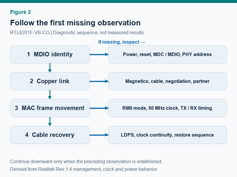
If identifier reads fail, stay with power, reset, the stable clock, the management pins, and the address straps. If identifiers are stable but link does not form, inspect the copper path and negotiation. The RSET resistor belongs in that review: its specified 2.49 kΩ value and 1% tolerance establish the transmit bias, and Realtek recommends keeping the circuitry away from interfering clock and signal traces. [1, §8.7]
If link is up but the MAC sees no frames, examine the RMII configuration and signal path rather than treating the LED as proof that the digital interface works. Check whether the host is actually transmitting data and whether receive activity reaches its pins. The PHY does not configure the host's DMA or network stack, so those layers need their own evidence after the physical interface is established.
Cable recovery is the final everyday behavior to test, not an optional stress test. Observe the reference clock while the cable is absent if the PHY owns that clock. Then confirm which state survives or changes during reconnection and reset. LDPS, full power-down, Energy Efficient Ethernet, and Wake-on-LAN are different mechanisms with different controls; grouping them under one “low power” switch makes the resulting behavior hard to explain. [1, §§8.5, 8.11–8.13]
A replacement discussion should start with what the new design needs to change. Package accessibility, a smaller RMII-only footprint, or an industrial temperature range can each justify looking beyond the main device. None of those goals is satisfied merely by finding another PHY whose description says 10/100 Mbps.
Table 5. Four related PHY candidates and the changes they imply
| Related MPN | Verified relationship or distinction | Boundary for a design review |
|---|---|---|
| RTL8201FL-VB-CG | Same documented Realtek family; 48-pin LQFP; MII/RMII | Different footprint and pin map; recheck shared-pin functions and layout |
| RTL8201FN-VB-CG | Same family; 48-pin QFN; MII/RMII; three LEDs in the selection table | Different package and supply/control details; do not copy the F circuit blindly |
| LAN8720A-CP-TR | Microchip 10/100 RMII PHY; 24-pin QFN; commercial ordering option | RMII-focused alternative requiring new pin, clock, power, and driver review |
| DP83848IVV/NOPB | Texas Instruments 10/100 PHY; MII/RMII; 48-pin LQFP; industrial −40°C to +85°C | Different electrical and package implementation; temperature capability does not establish compatibility |
Sources: Realtek Rev.1.4 Tables 59–60; Microchip LAN8720A/LAN8720Ai datasheet ordering information; TI DP83848IVV/NOPB official part details and datasheet. These are related candidates, not verified drop-in replacements. [1–4]
The FL and FN comparisons are useful because they remain close to the main device's functional family while exposing how much a package change can affect the board. The FN's regulator-control and LED options deserve their own reading. The word “family” saves some research; it does not remove the need to select the correct column in the pin and feature tables.
The Microchip option is relevant when a compact RMII interface is the design priority. Its exact commercial code should not be confused with the industrial LAN8720Ai naming used in the same document. The TI part addresses a different temperature and package requirement. Its documented interface features make it worth evaluating, but its clock circuit and register behavior must be taken from TI's own material rather than inherited from the Realtek initialization.
When discussing the part with YG GROUP, include the complete RTL8201F-VB-CG code, the intended MAC, the reference-clock owner, and the operating-temperature requirement. Those details turn a generic PHY inquiry into a useful component conversation. This article does not establish current stock, price, delivery time, or the qualification of a replacement on an existing PCB.
A reliable bring-up plan for this PHY begins with a small set of explicit decisions: the exact package, the sampled straps, the clock owner, and the reset sequence. The device's LDPS restriction gives those decisions a practical connection. Once the MAC depends on the PHY's reference output, a power-setting change can become an interface change. Keep that dependency visible, and the path from a management response to repeatable Ethernet traffic becomes much easier to follow.