
Jolin Zeng




| Picture | Part Number | Manufacturer | Stock | Action |
|---|---|---|---|---|
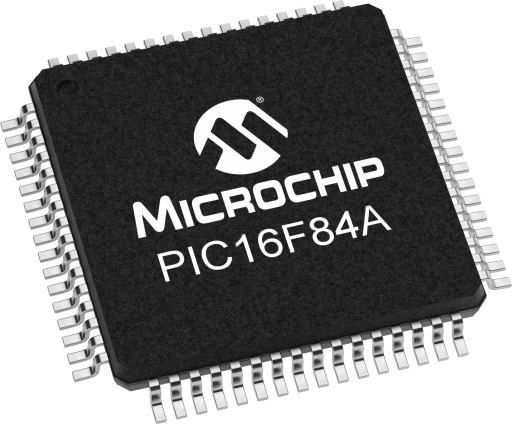 | PIC16F84A-04I/P | Microchip | 9,740 | |
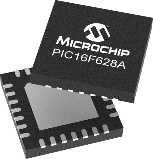 | PIC16F628A-I/P | Microchip | 9,810 | |
 | PIC16F648A-I/P | Microchip | 7,690 | |
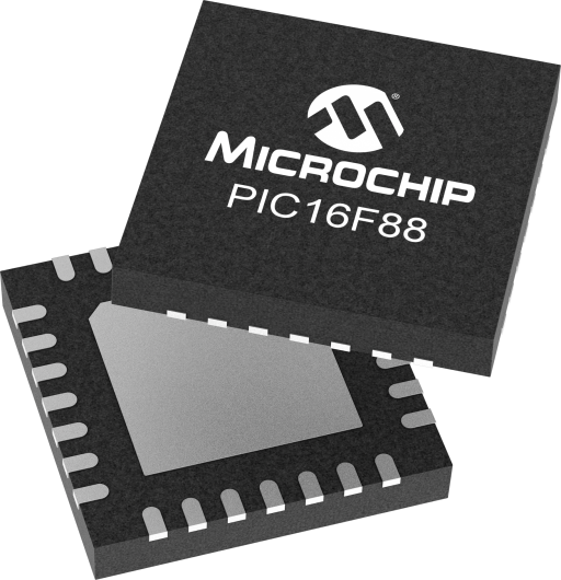 | PIC16F88-I/P | Microchip | 8,250 | |
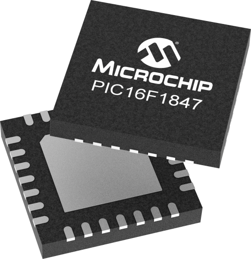 | PIC16F1847-I/P | Microchip | 7,280 |
Hardware clears WR and sets EEIF when the byte write completes. EEIF must be cleared in software, so a stale flag must not acknowledge the next operation. Associate completion with the pending address and expected value, then read the byte back. A multi-byte configuration still needs a separate record-validity decision before the application reports that it is saved.
No. The supplied DS35007C lists 4 ms typical and 8 ms maximum for a byte erase/write cycle. Typical timing is not a completion guarantee. Poll the documented state or use the completion interrupt with a bounded fault path. Include firmware overhead and verification in the record timing budget.
No. WREN permits write initiation, and clearing it after initiation does not stop the active cycle. WR is cleared by hardware on completion; software cannot cancel the operation by clearing that bit. Keep WREN disabled when updates are not intended, but use record recovery and qualified power behavior to handle interruption.
Category: Manufacturer Insights
Author: Jolin Zeng
Manufacturer: Microchip
A PIC16F84A-04I/P can finish an EEPROM byte write without finishing the configuration update that the application intended. That distinction matters when a controller stores a calibration value, counter or operating mode across several bytes. Firmware must first observe the device's write-completion state, then validate the stored record, and finally decide what to recover after reset. A delay that usually works on the bench does not establish any of those three conditions.
Microchip's DS35007C gives the useful starting points: 64 bytes of data EEPROM, a specific write-unlock sequence, hardware-controlled completion, and a write-error flag with a defined reset meaning. It also states that the power-on reset circuit does not generate an internal reset when the supply falls. A reliable settings store therefore needs both correct register handling and a deliberate response to interrupted power.
This guide applies those facts to the exact industrial, 4 MHz, PDIP order code. The proposed record format and test procedures are engineering examples derived from the documented behavior; they are not claims that this PIC implements transactional storage or that a particular board has passed power-failure testing.
The complete code matters before timing is discussed. In PIC16F84A-04I/P, the F device uses the standard supply range, 04 identifies the 4 MHz speed option, I denotes the industrial temperature range, and P identifies the PDIP package. The supplied datasheet even uses this exact code in its 18-lead PDIP marking example. Family headlines covering higher speed or lower voltage options should not replace those qualifiers.
No. WRERR has a defined meaning for writes prematurely terminated by MCLR reset or watchdog reset during normal operation. Its power-on value is unknown. Capture applicable reset evidence before initialization changes it, and validate stored records independently. The internal POR circuit does not generate a falling-supply reset, so supply supervision requires separate design review.
Two copies can preserve an older accepted record while another is updated, but the datasheet does not promise atomic multi-byte storage or anti-tearing. Invalidate and verify the destination first, verify its new contents, then commit and validate it. Qualify interruptions at every stage, checksum limitations and generation-counter wrap before accepting the recovery scheme.
At 5 V without a prescaler, the supplied watchdog table gives a 7 ms minimum timeout, while an EEPROM byte write can take up to 8 ms. Assuming the 18 ms typical watchdog period misses that overlap. Design watchdog service and bounded progress deliberately, and account for the prescaler shared with Timer0.
For a conventional 4 MHz XT design, use the PIC16F84A supply specification, not the PIC16LF84A row. The standard F device has a 4.0–5.5 V operating range for XT, RC and LP configurations in the supplied electrical table. That lower operating boundary is directly relevant to an EEPROM save: the data EEPROM read/write voltage row refers back to the minimum operating voltage. A processor that still appears to execute below that boundary is not evidence of specified operation.
Table 1: Device facts that constrain the save operation
| Item | Documented basis for this design | Practical consequence |
|---|---|---|
| Exact order code | PIC16F84A-04I/P; 4 MHz option; industrial −40 to +85°C; 18-lead PDIP | Preserve all suffixes when comparing boards or replacement stock |
| Data EEPROM capacity | 64 bytes, addresses 00h through 3Fh | Budget metadata and recovery copies before assigning payload addresses |
| Program and working memory | 1024 words of 14-bit program Flash; 68 bytes of data RAM | Avoid assuming enough RAM for several complete buffered records |
| Supply, XT configuration | Standard F device: 4.0–5.5 V | Hold execution within the applicable operating range during a save |
| EEPROM erase/write time | D122: 4 ms typical, 8 ms maximum | Observe completion; budget worst-case time rather than a typical delay |
| EEPROM endurance | D120: 1 million minimum erase/write cycles at 25°C, 5 V; 10 million typical | Treat the stated conditions and the most frequently written cell explicitly |
Source: Microchip DS35007C, pp. 1, 13–14, 49, 52, 55, 69 and 87. Typical figures are design guidance, not tested limits. Table compiled by YG GROUP.
The operating temperature range does not turn the room-temperature endurance entry into a lifetime guarantee at every industrial temperature. Likewise, program Flash endurance is a different specification from data EEPROM endurance. Keep these memories separate in requirements, source notes and calculations. An attractive endurance number is of little use if the application rewrites a status byte much more often than the payload it protects.
A useful save interface distinguishes a request accepted into RAM, a byte operation started, a byte verified, and an entire record accepted for recovery. These events can occur at different times. If the user interface displays “saved” as soon as WR is set, a supply interruption can leave the previous settings, a partial update or an invalid record even though the interface appeared to acknowledge success.
For a small controller, the interface can be a simple state variable rather than a complicated storage library. The foreground code snapshots the requested settings, gives one routine ownership of the EEPROM registers, and reports completion only when the agreed record checks pass. A second request must be rejected, queued or coalesced according to an explicit rule. It must not overwrite EEADR or EEDATA while another operation is being prepared.
Snapshot consistency also deserves attention. Suppose an interrupt updates a two-byte measurement while the foreground copies it into the pending record. The copied bytes can describe different measurement instants before EEPROM writing even begins. Protect the RAM snapshot with an appropriately short critical section, then release that protection before the millisecond write interval. Correct storage cannot repair a record assembled from inconsistent source data.
Choose recovery behavior with the application's output behavior in mind. A display preference can usually fall back to a default. A calibration coefficient controlling an actuator may require an inhibited output and a visible fault instead. The validation routine should return both the selected data and the reason for selection, so the rest of the application can distinguish a normal boot from recovery using an older record.
Data EEPROM is accessed indirectly through EEADR, EEDATA, EECON1 and EECON2. The address and data registers are in Bank 0; the control registers are in Bank 1. EECON2 participates in the unlock sequence but is not a physically implemented storage register that software can read back to confirm a password. Bank selection is therefore part of the driver, not background context that callers should happen to establish.
Before starting a byte, confirm that the previous write is no longer active and clear any completion indication retained by software from that operation. Load the target address and new byte, then enable writing with WREN. The required unlock sequence writes 55h to EECON2, writes AAh to EECON2, and sets WR. Microchip strongly recommends disabling interrupts during this sequence. An inserted call, bank change or compiler-generated instruction must not break the required ordering.
Table 2: Register state and software responsibility
| Register or bit | Hardware meaning | Driver responsibility |
|---|---|---|
| EEADR | Selects the EEPROM byte | Constrain addresses to the intended 00h–3Fh map |
| EEDATA | Holds the read or write byte | Preserve the expected value separately for verification |
| EECON2 | Unlock-sequence destination | Write 55h then AAh immediately before initiating the write |
| WREN | Allows write initiation; not cleared automatically | Enable only around intended updates and clear when no further write is needed |
| WR | Starts the write; hardware clears it on completion | Never treat a software attempt to clear WR as cancellation |
| EEIF | Hardware sets it when the write completes | Clear stale flags and acknowledge the completed operation in software |
| WRERR | Reports specified prematurely terminated writes | Interpret with reset context; do not treat it as a universal power-failure detector |
Source: Microchip DS35007C, Section 3 and Table 3-1. Table compiled by YG GROUP.
Once the write has started, clearing WREN does not stop that write. This is useful for keeping subsequent writes disabled, but it is not an emergency-abort facility. Restore the caller's previous interrupt state after the protected sequence; blindly enabling global interrupts is wrong when the caller intentionally entered with them disabled. Review generated assembly when a C helper is used, particularly around bank changes and the unlock instructions.
The write itself is timed inside the device. At a 4 MHz oscillator frequency, the instruction-cycle relation gives a 1 µs cycle, while the EEPROM operation takes milliseconds. There is normally no reason to keep interrupts disabled for the entire write interval merely to protect the unlock. Instead, prevent other execution paths from taking ownership of the EEPROM interface while allowing unrelated time-critical work to continue.

Figure 1: Conceptual driver sequence for one EEPROM byte. The short unlock critical section and the longer hardware write interval have different purposes. Clear WREN when appropriate and restore the prior interrupt state after initiation. Source: Microchip DS35007C, Section 3. Diagram: YG GROUP.
WR clearing tells software that the active byte write has completed. EEIF provides a completion event that can be polled or used with the EEPROM interrupt enable and global interrupt enable. The flag still needs software acknowledgement. If a previous EEIF remains set, polling it immediately after starting another byte can falsely report that the new byte has already finished.
A polling implementation should have an explicit pending state and a bounded fault path. Observe WR until hardware clears it, then perform readback before advancing the record writer. A timeout is a diagnostic result, not permission to force WR low or immediately start another write. Capture the state needed to investigate supply, clock, reset and software ownership, then return a failure that the application can handle without claiming persistence.
An interrupt-driven implementation needs the same ownership discipline. The interrupt handler acknowledges EEIF and updates the driver's state; it should not let multiple callers independently launch the next byte. Keep the expected address and value associated with that pending operation. A flag says a write ended, but it does not identify the application's record or prove that its source buffer remained unchanged.
For readback, select the address, set RD, and obtain the result from EEDATA as documented. Compare against the expected byte before reusing that expected-value storage. If verification fails, preserve the old valid record and report a failed update. Repeated blind retries can hide a hardware fault and increase wear. A small, bounded retry policy may be appropriate only when the application defines its purpose and records the failure.
Readback is valuable evidence of the immediate stored value. It does not prove long-term retention, validate the meaning of a calibration coefficient, or turn several byte writes into one indivisible transaction. Those are different checks and should remain visible in both the driver interface and the qualification plan.
The 4 ms typical EEPROM write time is an unsuitable fixed completion delay. The supplied table gives 8 ms maximum for the byte erase/write operation. Firmware overhead, verification and record management add time beyond that operation. A save of many bytes can therefore be long relative to a small controller's control loop, even when each individual write behaves correctly.
The watchdog creates a particularly useful boundary check. At 5 V with no prescaler, DS35007C lists a watchdog timeout of 7 ms minimum, 18 ms typical and 33 ms maximum. The minimum watchdog interval is shorter than the maximum EEPROM write interval. A design that assumes an 18 ms watchdog and blocks for one supposedly safe write can reset under a permitted combination of conditions.
Service the watchdog through a deliberate, healthy-progress policy, or select a suitable watchdog prescaler arrangement and validate the resulting timing. Do not hide a stuck storage state by clearing the watchdog forever in an unbounded wait loop. Timer0 and the watchdog share the prescaler, so changing its assignment affects another part of the system and has a documented switching sequence. Review that interaction as part of the firmware configuration rather than changing it locally inside every save.
Supply hold-up is a separate calculation. As an illustrative lower-bound estimate, a constant 10 mA load needing 10 ms across a usable 0.5 V drop requires C = I × t / ΔV = 200 µF. The current, interval and voltage drop here are assumptions, not PIC16F84A measurements or a capacitor recommendation. Effective capacitance, tolerance, ESR, leakage, regulator behavior and every attached load must be included before hardware is selected.
The usable voltage interval must end above the applicable operating boundary, with margin for the detection threshold and its tolerance. A larger capacitor does not help if firmware notices failure too late, if another load drains the rail, or if MCLR is asserted before the intended save can complete. Decide whether the product needs a last-moment save at all. Saving deliberate changes while power is healthy and retaining an older valid record is often easier to verify.
WRERR has a narrower meaning than “some power event happened.” The datasheet defines it for a write prematurely terminated by MCLR reset or a watchdog reset during normal operation. Its power-on reset value is unknown. That makes it useful diagnostic evidence in a qualified reset path, but unsuitable as the only test of EEPROM validity at every boot.
EEADR and EEDATA remain unchanged for the non-power-on resets shown in the register reset table, whereas their power-on values are unknown. If recovery software intends to use those retained registers, it must capture them before initialization overwrites them and before it changes the relevant reset-status evidence. A clean power-on path must not retry an address and byte merely because the registers happen to contain plausible values.
Table 3: Reset observations and appropriate recovery decisions
| Event or observation | What can be inferred | What must still be checked |
|---|---|---|
| MCLR interrupts a write during normal operation | WRERR can indicate the interrupted operation; address/data registers are retained as specified | Capture evidence early, establish stable power and validate the complete record |
| Watchdog interrupts a write during normal operation | The write may be terminated; timeout evidence helps diagnose firmware timing | Investigate watchdog scheduling and do not repeatedly replay a failing update |
| Power-on reset | EEPROM control and working-register startup states follow the reset table | Do not rely on WRERR, EEADR or EEDATA as a trustworthy pending transaction |
| Supply falls without effective external reset control | Internal POR does not itself generate a falling-supply reset | Ensure execution and writing cannot continue outside the specified supply range |
| Both records appear invalid at boot | No record has passed the application's acceptance rules | Use a defined default or fault state and keep outputs appropriate to that state |
Source: Microchip DS35007C, pp. 13–14 and 24–26. Recovery decisions are engineering guidance from YG GROUP.
Capture reset information early enough that instructions such as CLRWDT do not erase the evidence needed for diagnosis. Keep this early capture small and deterministic, then perform the slower record scan after the basic execution environment is established. The record validator should work even when the reset cause is ambiguous: valid data is accepted because its structure and checks pass, not because the reset flag happened to look reassuring.
The falling-supply limitation is especially important on an older control board. Power-on reset, the power-up timer and oscillator startup delay describe startup behavior; they do not provide an undocumented brownout-reset feature. Where the supply can decay or dip, evaluate external supervision and the MCLR network against the actual operating limits. Verify the voltage at the MCU pins rather than assuming the bench supply display describes the local rail.
Consider an example that divides the 64-byte EEPROM into two 32-byte slots. Each slot contains a format identifier, payload length, generation counter, payload, checksum and commit marker. One possible allocation uses one byte each for format, length and generation, 26 payload bytes, a two-byte checksum, and one commit byte. This is a proposed software layout, not a manufacturer-defined memory format.
The current valid slot stays untouched while the other slot is prepared. First invalidate the destination slot's commit marker, complete and verify that operation, and only then change its record contents. Write the new metadata, payload and checksum with per-byte completion handling. Read back and validate the header, payload and checksum before writing the final commit marker; this pre-commit check must not require a valid marker yet. Include the format, length and generation fields as well as the payload in checksum coverage. After the commit byte completes, validate the whole slot again before acknowledging the save.

Figure 2: Illustrative two-slot allocation across addresses 00h–3Fh. The destination is not accepted until its structure, checksum and final marker pass validation. This design reduces exposure to partial updates; it is not a documented atomic-write or anti-tearing guarantee. Diagram: YG GROUP.
Invalidating the destination before rewriting matters because a previously valid marker could otherwise survive while the rest of that slot is partially replaced. Verification of the invalidation also prevents firmware from proceeding after a failed attempt to retire the old contents. The untouched source slot supplies the fallback during the update, so there is no need to destroy it merely to announce that a newer record exists.
On boot, scan both slots. Check format, length bounds, checksum, marker and application-specific value ranges. If only one slot passes, select it. If both pass, compare generation values using a documented wrap rule. A one-byte generation counter wraps after 255; ordinary unsigned “larger is newer” comparison fails at that boundary. With only adjacent retained generations, a modular comparison can be defined, but ambiguous differences should have a deterministic fault or tie policy.
A checksum does not eliminate every possible corruption pattern, and an interrupted byte write is not promised to produce one predictable value. Test the chosen marker and validation scheme under power cuts at every update stage, including invalidation and final commit. If the required failure model is stronger than this arrangement can demonstrate, the design may need different storage hardware, more independent metadata, or tighter supply supervision.
Also decide how factory defaults and schema changes enter this process. A firmware update might interpret the same payload bytes differently. Including a format identifier allows the boot code to reject or migrate an old layout deliberately. Do not rewrite both slots with new defaults at every boot; that consumes endurance and can discard a valid calibration before the application has explained why it was rejected.
Endurance should be calculated for the busiest physical byte. In the two-slot example, each destination commit marker is written once to invalidate and once to commit during that slot's update. Its wear rate can therefore exceed that of a payload cell. Alternating slots does not automatically multiply the whole system's lifetime by two when metadata receives extra writes.
At one write per second to a single cell, one million operations represents about 11.6 days. At one write per minute, it represents about 1.9 years. These are arithmetic translations of a cycle count, not predicted product lifetimes: the endurance entry has stated temperature and voltage conditions, and the actual workload and failure criteria still matter. The calculation is useful because it makes an unnecessarily frequent save policy visible.
Coalesce repeated setting changes, save only when a value has meaningfully changed, and distinguish a live counter from a durable checkpoint. A user turning a knob through fifty intermediate positions may need only the final settled setting stored. If a counter must survive every event, calculate whether this EEPROM and record format suit that requirement instead of silently weakening the persistence promise in software.
A different PIC may be worth investigating when EEPROM capacity, reset handling or peripheral requirements outgrow the existing design. A familiar package outline is only the beginning of that review. Firmware initialization, pin functions, oscillator configuration, programming tools and persistence semantics all need their own comparison. None of the following exact codes is asserted to be a drop-in replacement.
Table 4: Four exact Microchip models for a migration study
| Exact model | Relationship to the present controller | Main review task | Compatibility boundary |
|---|---|---|---|
| PIC16F628A-I/P | Another PIC16 device for a small control-board redesign | Compare peripheral initialization, EEPROM handling and reset configuration | Rebuild and test firmware; do not transplant the existing binary |
| PIC16F648A-I/P | A distinct member of the PIC16F627A/628A/648A family | Evaluate the required memory map and application growth separately from package fit | Verify actual pin use, programming and electrical limits |
| PIC16F88-I/P | A separate PIC16 family candidate | Reassess multiplexed pin functions and startup configuration | Similar physical form does not establish identical default behavior |
| PIC16F1847-I/P | A further PIC16 architecture option for a broader redesign | Review the core, peripheral setup and nonvolatile-storage driver together | Treat this as a port with new qualification, not an EEPROM repair shortcut |
Sources: the linked Microchip product pages and Microchip catalog-part attachment PCN_CYER-16AOEB180. The attachment establishes exact code identity, not current stock, lifecycle or interchangeability. Table compiled by YG GROUP.
The present article adopts the PIC16F84A datasheet for quantitative behavior. The alternatives are a bounded research shortlist supported by official product identities; their full electrical specifications are not substituted into the existing design. Before choosing one, obtain its applicable datasheet and errata, match every used pin and configuration bit, and repeat the same interrupted-write qualification with the new driver.
Start with a repeatable healthy-power save and record its expected byte sequence, completion handling and boot result. Add a diagnostic output that marks the state under test without changing the storage policy. Observe local VDD, MCLR and that diagnostic signal together. A power-cut command issued by a test fixture is not the same instant that voltage at the MCU crosses its operating boundary.
Table 5: A focused EEPROM qualification matrix
| Test condition | Evidence to capture | Required application result |
|---|---|---|
| Normal byte and record write | Address, expected byte, WR/EEIF handling and final readback | One acknowledged record that passes all acceptance checks |
| Interrupt load during initiation | Generated unlock instructions and timing under worst scheduled load | Correct unlock order with the previous interrupt state restored |
| Watchdog near a write boundary | Reset evidence and elapsed time through the storage state machine | No false success; bounded recovery and a diagnosable timeout cause |
| MCLR during each update stage | Interrupted stage and both slots after restart | Previous valid record or a defined fault/default path |
| Controlled supply removal and dips | Local rail decay, reset timing and recovered record contents | No acceptance of an invalid or out-of-range record |
| Generation wrap and malformed records | Both slots around wrap; invalid length, format and checksum cases | Deterministic selection without reading outside the allocated map |
Source: proposed engineering verification plan by YG GROUP, derived from DS35007C behavior. These are test requirements, not reported test results.
Sweep interruption time across the whole update, rather than cutting power once near the middle. Include the last commit byte, the interval after completion but before acknowledgement, and the next boot's record selection. Repeat with the intended temperature and supply conditions and with representative load changes. Keep test firmware, compiler configuration, record format and captured traces together so another engineer can reproduce a failure.
The acceptance criterion should be written before testing: after every qualified interruption, the controller either selects a record that passes the specified checks or enters its documented recovery state. A missing “saved” acknowledgement may still leave a valid new record; the application should handle that possibility without applying an event twice. For PIC16F84A-04I/P, this explicit contract makes WR, EEIF, WRERR and readback useful parts of a complete persistence design.