
Kelsey Lee




| Picture | Part Number | Manufacturer | Stock | Action |
|---|---|---|---|---|
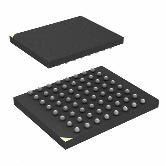 | PC28F256P33BFE | Micron | 6,530 | |
 | PC28F256P33TFE TR | Micron | 1,080 |
They are at the bottom of the array: four 32 KiB blocks covering byte offsets 0x00000000–0x0001FFFF under the single-x16-device mapping used here. The next block begins at 0x00020000. [1, p. 11]
The diagram uses word addresses. The last 16-bit word occupies byte offsets 0x01FFFFFE and 0x01FFFFFF. Confusing those units makes the apparent capacity half the actual 32 MiB array. [1, pp. 11, 15]
No. Its small blocks are at the top, and its device identifier differs. Software and the update layout must account for those differences before a replacement can be considered. [1, pp. 11, 27]
No. The designation identifies the parameter-block location. Micron separately describes block locking, lock-down and WP# behavior. All blocks start locked, but the documented software and hardware mechanisms determine whether a block can subsequently be modified. [1, p. 35]
By Kelsey Lee | 20 September 2026
PC28F256P33BFE is Micron's 256 Mb P33-65 nm parallel NOR device with a bottom-parameter-block organization. Its four small erase blocks occupy the lowest 128 KiB of a 32 MiB array. The key firmware detail is that Micron's memory-map figure uses 16-bit word addresses: convert those offsets before comparing them with a byte-addressed linker map or update image. [1, pp. 2–3, 11]
The complete PC28F256P33BFE identifier appears in Micron's standard-parts table. That table identifies it as the 256 Mb bottom-boot tray option. The part-number decoder identifies PC as the lead-free 64-ball Easy BGA package and B as the bottom-parameter location. The related PC28F256P33TFE is the top-boot tray option. Both are documented parts, but their small erase blocks are at opposite ends of the address space. [1, pp. 2–3]
That difference matters even when an image can be read from either device. A software partition is only a range of addresses; the flash erase operation acts on a physical erase block. An updater that assumes a small block exists at the bottom of a top-boot device can erase a larger range than its author intended.
For this reason, keep the complete MPN in the bill of materials, programmer profile and firmware compatibility record. A family-level label such as “256 Mb P33” loses the parameter-location information. The datasheet also cautions that inclusion in its part table does not establish current orderability. No present supply or lifecycle claim is made here. [1, p. 2]
**Figure 1. Keep word addresses separate from byte offsets.** Calculated PC28F256P33BFE erase-region map for one x16 device mapped contiguously onto a byte-addressed host, with no lane interleaving. Inclusive word ends convert to 2 × end + 1. The main region starts at byte offset 0x00020000. Blocks are drawn schematically, not in proportion; add the host base address separately. Sources: [supporting source 1](https://pdf.icgoo.net/productinfo/allpdf/3a8593fe-e247-3931-ad42-a99741a070c5.pdf). **Figure 2. Erase-time planning needs the maximum.** Micron lists the same 0.8 s typical and 4.0 s maximum erase times for the 32 KiB parameter and 128 KiB main blocks. Typical values are qualified at nominal voltages and 25°C case temperature, exclude system overhead and carry the source’s sampling qualification. Four sequential erases give a calculated 16 s device-erase budget before programming, software overhead and verification; this is not a benchmark or a complete timeout recommendation. Sources: [supporting source 1](https://pdf.icgoo.net/productinfo/allpdf/3a8593fe-e247-3931-ad42-a99741a070c5.pdf).Micron's 256 Mb memory map is labeled A[24:1] and its Easy BGA ballout identifies A1 as the least significant device address bit. Each addressed array word contains 16 bits. [1, pp. 11, 15] For a single x16 device mapped contiguously onto a byte-addressed host, the corresponding byte offset is twice the device word offset.
Use this relationship only after confirming how the host memory controller connects and maps the bus. The following examples assume one x16 device, no lane interleaving and a contiguous mapping. They are address calculations, not a tested configuration for a particular processor.
For an inclusive word range from Wstart to Wend:
first byte offset = 2 × Wstart
last byte offset  = 2 × Wend + 1
If the flash begins at host base address B, add B to those offsets. Keep the base-address addition separate from the word-to-byte conversion; doing both implicitly inside a driver makes a factor-of-two error harder to spot.
Micron labels the small blocks as 16 Kword and the main blocks as 64 Kword. These correspond to 32 KiB and 128 KiB respectively. This article uses KiB for 1,024 bytes and MiB for 1,048,576 bytes to make the units explicit; those are the binary sizes represented in the manufacturer's map. [1, p. 11]
The bottom-boot map has four 16 Kword parameter blocks followed by 255 main blocks of 64 Kword. The table below converts selected manufacturer word ranges into byte offsets relative to the start of one device. It is an editorial calculation from Micron's Figure 2, not a separate manufacturer memory map. [1, p. 11]
| Block or region | Device word addresses, inclusive | Byte offsets, inclusive | Erase-block size |
|---|---|---|---|
| Parameter block 0 | 0x000000–0x003FFF | 0x00000000–0x00007FFF | 32 KiB |
| Parameter block 1 | 0x004000–0x007FFF | 0x00008000–0x0000FFFF | 32 KiB |
| Parameter block 2 | 0x008000–0x00BFFF | 0x00010000–0x00017FFF | 32 KiB |
| Parameter block 3 | 0x00C000–0x00FFFF | 0x00018000–0x0001FFFF | 32 KiB |
| First main block, block 4 | 0x010000–0x01FFFF | 0x00020000–0x0003FFFF | 128 KiB |
| Last main block, block 258 | 0xFF0000–0xFFFFFF | 0x01FE0000–0x01FFFFFF | 128 KiB |
The capacity check is straightforward: four times 32 KiB plus 255 times 128 KiB equals 32 MiB. There are 259 physical erase blocks in total. The first main block begins at byte offset 0x00020000, not 0x00010000. Copying the latter directly from the word-address diagram would place a byte-addressed partition in the third small block.
An engineering review should compare three artifacts in the same units: the flash driver geometry, the linker or partition map, and the programmer's address interpretation. If one uses words and another uses bytes, label that difference at the interface rather than relying on an undocumented convention.

The Common Flash Interface provides another way to examine the device geometry. Micron explains that CFI offsets for this x16 device are word addresses, and that the returned CFI byte is on DQ[7:0], with zero on DQ[15:8]. The QRY signature starts at word offset 0x10. Under the single-device byte-addressed assumption above, its first word is read at byte offset 0x20 relative to the mapping base. [1, pp. 49–50]
The CFI geometry tables give a size exponent of 0x19 for the 256 Mb device. Calculating 2^25 yields 33,554,432 bytes, or 32 MiB. They also identify two erase regions. The region descriptor encodes the block count minus one and a block size in units of 256 bytes. For the bottom-boot device, the first descriptor therefore decodes to four blocks of 32,768 bytes; the second decodes to 255 blocks of 131,072 bytes. [1, pp. 52–53]
This creates a useful review loop. Decode the returned geometry, compare it with the expected complete-part profile, and only then let update software use its block boundaries. A successful QRY read demonstrates that the command/read path is working for that query; it does not by itself validate all hardware timing or prove the provenance of a purchased component.
Avoid hardcoding only the total capacity. Two devices can expose the same array size while requiring different erase-region ordering. A driver that checks density but ignores region descriptors can still use the wrong map.
PC28F256P33TFE is useful as a close comparison because the manufacturer lists it alongside the primary device. In its top-boot organization, the four small parameter blocks occupy the last 128 KiB. Their combined byte range is 0x01FE0000–0x01FFFFFF, calculated from the top-boot word map. The lower portion instead consists of 128 KiB main blocks. [1, pp. 3, 11]
| Review item | PC28F256P33BFE | PC28F256P33TFE |
|---|---|---|
| Manufacturer table configuration | Bottom boot, tray | Top boot, tray |
| Small-block location | Lowest 128 KiB | Highest 128 KiB |
| Lowest erase block | 32 KiB | 128 KiB |
| Highest erase block | 128 KiB | 32 KiB |
| Device identifier in Table 11 | 0x8922 | 0x891F |
Source: Micron standard-parts table, memory map and device-ID table. [1, pp. 3, 11, 27]
These differences make the top-boot part a comparison reference, not an automatically approved replacement. A replacement assessment must check the actual boot mapping, update layout, software identification behavior, package implementation and applicable electrical requirements. Sharing a family name does not resolve those system dependencies.
A small logical record does not imply a small physical update. Micron specifies block-level erase: the addressed block is the unit affected by that operation. [1, p. 33] If boot code and a changing configuration record share a physical block, an erase intended for the record also affects the code in that block.
For an original planning example, suppose a configuration region occupies byte offsets 0x00018000–0x0001FFFF on PC28F256P33BFE. That region coincides with parameter block 3. Moving its start upward or downward without reviewing the new physical boundaries may cause it to share a block with other data. The address table supplies the geometry; the decision to allocate that region to configuration data belongs to the system design.
A robust map records each partition's first byte, length, physical erase blocks and update owner. If a partition contains several blocks, the update routine should enumerate the actual geometry rather than assume one erase size throughout the array. The transition at byte offset 0x00020000 deserves an explicit boundary test.
For boot recovery, document which image remains executable during an interrupted update, which data is changed first and how software decides that an update is complete. Those are application design requirements. The flash's erase map alone does not guarantee a recoverable update scheme.
The device's write buffer holds up to 512 words, and buffered programming cannot cross an erase-block boundary. Micron also gives alignment restrictions and describes a reduced maximum buffer size for a misaligned range crossing a 512-word boundary. [1, pp. 28–29] A driver should split transfers using both the programming-buffer constraints and the current physical erase block; treating either constraint as the only boundary is insufficient.
The command sequence itself matters. After the buffered-program setup command, the device already supplies status data on reads. Micron specifically warns against inserting a READ STATUS REGISTER command at that point because it is interpreted as the word count. [1, p. 63] This is an example of why a generic “poll status” helper needs to know the command phase, not merely the device family.
Ready is also different from successful. The status register includes error and protection information in addition to its ready bit. Check the complete relevant status, preserve useful failure information, and clear errors at the documented point before proceeding. Return the device to array-read mode before treating reads as image contents. [1, pp. 20, 28, 38–39]
There are editorial inconsistencies elsewhere in this datasheet: its erase prose contains conflicting bit-polarity wording, and the status-flowchart labels do not consistently match the explicit status table. For firmware implementation, reconcile the applicable command description and register definition and obtain manufacturer clarification for any unresolved conflict. Do not copy an isolated flowchart into a production driver. The block geometry used in this guide is consistent across the memory map and CFI tables. [1, pp. 11, 33, 38, 52–53, 70]
After power-up or reset, the device defaults to asynchronous array-read mode. Micron cautions that resetting the CPU without resetting the flash can leave the processor reading status information instead of array data. Its reset guidance therefore connects flash reset behavior with CPU initialization. [1, pp. 19, 71]
This is directly relevant to a boot-block investigation. A correct address map cannot make status-register contents into valid instructions. When a board boots only after a full power cycle, inspect the command state and reset relationship as well as the image placement.
Reset during an active program or erase can terminate the operation and leave the affected location or block invalid. [1, p. 19] Include that condition in the recovery design and validation procedure. It should not be treated as a benign way to exit every update state.
Small blocks reduce the amount of data affected by an erase; they do not guarantee proportionately shorter erase latency. Micron's table lists both the 32 KB parameter block and the 128 KB main block with a typical erase time of 0.8 seconds and a maximum of 4.0 seconds. The table qualifies typical values at nominal voltages and a case temperature of 25°C, excludes system overhead and notes the sampling basis. [1, p. 91]
For an illustrative four-block update performed sequentially, four times the 4.0-second device maximum equals 16 seconds of erase time before programming, software overhead or verification is included. This is a planning calculation from the table, not a benchmark or a complete application timeout recommendation. The actual timeout policy must account for the chosen command sequence and system behavior.
This distinction is valuable for watchdog design. A timeout derived only from the typical value can reject a permitted slower operation. Conversely, simply increasing the timeout will not fix an address error, a locked block or an invalid programming supply.

p33_65nm_MLC_256Mb-512mb.pdf, Rev. D, February 2018, 92 pages. Manufacturer author: Micron; public mirror host: ICgoo. Manufacturer-authored datasheet, Rev. D. This historical document does not establish current availability or lifecycle.