
Doris Lee




| Picture | Part Number | Manufacturer | Stock | Action |
|---|---|---|---|---|
 | MPM3833CGRH-Z | Monolithic Power Systems | 2,600 | |
| MPM3822CGRH-Z | Monolithic Power Systems | 2,110 | |
| MPM3830GQV-Z | Monolithic Power Systems | 8,690 | |
| MPM3820GQV-Z | Monolithic Power Systems | 2,110 | |
| MPM3840GQV-Z | Monolithic Power Systems | 3,670 |
No. MPM3833CGRH-Z integrates its power MOSFETs and a nominal 1 µH inductor. The board still needs the input and output capacitors and the feedback divider, plus any components required by the system's enable and sequencing arrangement. Integration reduces the power-stage component count; it does not remove the need for a short input return, a clean feedback path, and suitable thermal copper.
Do not make that assumption. The documented package identifies pins 17 and 18 as DNC and requires them to remain floating. Its land-pattern note also defines a central keep-out where PCB traces and vias must not connect electrically or mechanically. Follow the exact MPM3833C package drawing. Pin 11 is NC and has different instructions, so NC and DNC must remain distinct in the footprint review.
No. The broad low-ripple description does not establish that result for every board and operating condition. The Rev. 1.0 electrical table gives 5 mV typical ripple at a 3.6 V input, 1.2 V output, 22 µF output capacitance and 2 A load. Actual ripple at the load also depends on capacitance under bias, routing, return paths and measurement setup. Verify against the powered device's own rail requirements.
By Doris Lee
The MPM3833CGRH-Z from Monolithic Power Systems integrates the switching MOSFETs and inductor in a compact step-down module. It is a useful candidate for low-voltage optical-module rails, but low ripple still depends on the board around it. Start with the input capacitor return, protect the feedback path, and respect the package keep-out. Then measure ripple at the load under defined conditions before deciding whether the rail needs additional filtering.
Integrating the inductor removes one substantial placement decision. You no longer choose an external inductor, route a separate switch-to-inductor connection, or fit that component beside the converter. The input capacitor, output capacitor, feedback divider, and their return paths still belong to your design. Those connections determine how the module interacts with a sensitive load.
MPS lists optical modules, FPGA and ASIC supplies among the MPM3833C applications. That is a sensible starting point for a layout discussion: these systems can place a compact power stage close to circuitry that cares about rail disturbances. It does not establish compatibility with a particular optical transceiver, data rate, laser driver, or communications standard. Each load brings its own voltage tolerance, noise limits, sequencing requirements, and thermal environment. See the MPS MPM3833C product description.
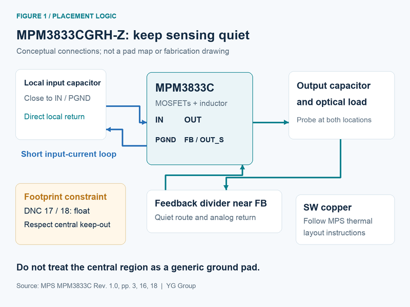
**Figure 1.** Organize the MPM3833CGRH-Z layout around a short input-capacitor loop and a separate, quiet sensing route. The drawing shows functional relationships, not pad geometry or a fabrication-ready footprint. Source: MPS datasheet pages 3, 16 and 18; illustration by YG Group. **Figure 2.** Use the observed symptom to choose the next measurement. Ripple, load response, distribution loss, and radiated emissions need different evidence. This is an editorial measurement workflow, not measured MPM3833CGRH-Z performance. Basis: MPS datasheet characterization and application sections.No. PG is open-drain but includes a nominal 440 kΩ internal pull-up to IN. Its high state therefore needs to be checked against the receiving pin's voltage limits and all power-sequencing states. An external pull-up or level-interface arrangement must be reviewed with that internal path present. PG also reports a comparatively broad regulation window; it does not prove compliance with a tighter noise or voltage-tolerance requirement.
First verify the measurement with a short probe connection and compare the output-capacitor node with the actual load point. Pickup, real switching spikes, periodic ripple and load-step droop call for different investigations. An added bead and capacitor can help in a selected band, but they also change impedance, DC drop and transient behavior. Confirm the sensing topology and validate the modified network instead of treating filtering as a universal fix.
The related MPM3822CGRH-Z, MPM3830GQV-Z, MPM3820GQV-Z and MPM3840GQV-Z are comparison candidates, not qualified replacements. They differ in current capability, package, input range or operating behavior. Even a similar body size does not establish matching pin functions or identical dynamic behavior. Compare the exact electrical limits, land pattern, sequencing and thermal requirements, then validate the intended circuit before approving a substitution.
The exact part here is MPM3833CGRH-Z, supplied in the QFN-18 package described as 2.5 × 3.5 × 1.6 mm. The ordering page of the supplied Rev. 1.0 datasheet identifies MPM3833CGRH and adds the -Z suffix for tape-and-reel. Keep that identity attached to the schematic symbol and purchasing record. A similar module name or package outline alone is not enough to justify reusing a footprint.
Table 1. Design facts that affect the first placement pass
| Item | Documented value or behavior | What it changes on the board |
|---|---|---|
| Recommended input | 2.75–6 V | Verify the voltage at the module during cable and load disturbances. |
| Output capability | Up to 3 A continuous | Check thermal conditions and distribution losses before allocating the full current. |
| Output adjustment | From 0.6 V; step-down operation | Select the divider for the rail and leave input-to-output headroom. |
| Integrated inductor | 1 µH nominal | External copper still affects switching-current paths and heat removal. |
| Operating mode | Forced continuous conduction mode | Characterize idle operation as well as full load. |
| Package | QFN-18, 2.5 × 3.5 × 1.6 mm | Use the exact land pattern and central keep-out instructions. |
Source: MPS MPM3833C datasheet, Rev. 1.0, pages 1–5 and 18. Current capability is subject to the application's electrical and thermal conditions.
A 5 V source feeding a 1.2 V rail is a useful example throughout this discussion. It is an illustrative operating point, not a complete optical-module reference design. The load has not been specified, and no board measurements are claimed here. The purpose is to make the placement and verification decisions concrete enough to review before fabrication.
Before drawing copper, write down where that 5 V comes from. A local upstream regulator, a backplane connector, and a long laboratory lead can all show the same DC voltage while presenting different impedances. The local bypass capacitor must support the switching stage at its pins. A large bulk capacitor several centimeters away does not give you the same short return path.
Also separate the voltage at the converter from the voltage at the load. A quiet output capacitor cannot compensate for every disturbance caused by a narrow trace, connector, or shared return farther downstream. Leave room to probe both locations. That small placement decision makes later debugging much more decisive.
Give the input capacitor a direct connection to IN and PGND. MPS specifically recommends an 0805 ceramic input capacitor close to the IC and instructs designers to connect its two ends directly to those pins. Treat this as a placement constraint, then arrange the lower-current signals around it. The recommendation appears in the datasheet PCB layout section on page 16.
The reason is the discontinuous input current of a buck converter. During part of the switching cycle the source supplies the power stage; during the other part it does not follow the same path. A local capacitor supplies much of that rapidly changing current. Extra trace length and a remote return add parasitic impedance exactly where the current changes quickly.
Look at the complete route, including the ground connection. A capacitor can sit next to the module yet connect through a thin trace to a distant ground via. In a placement screenshot it looks close; electrically the loop can still be long. Follow the path from the capacitor's positive pad into IN, through the internal switching stage, and back from PGND to the negative pad.
Table 2. Pin groups to keep distinct during routing
| Function | Pins in the documented package | Layout treatment |
|---|---|---|
| IN | 13, 14 | Short, broad connection to the local input capacitor. |
| PGND | 16 | Direct local capacitor return, connected into the ground structure. |
| OUT | 8, 9, 10 | Short connection to output capacitance and a suitable load-current route. |
| FB and OUT_S | 2 and 3 | Keep sensing paths away from switching copper; follow the application circuit. |
| AGND | 1 | Preserve a quiet reference for the feedback network. |
| SW | 5, 6, 7, 15 | Follow the manufacturer's layout and heat-spreading guidance. |
| DNC | 17, 18 | Leave floating; enforce the package keep-out. |
| NC | 11 | Float or connect to ground as allowed by the pin table; do not confuse with DNC. |
Source: MPS MPM3833C datasheet, pages 2–3, 16 and 18. This grouping is a routing aid, not a replacement for the package drawing.
The input capacitor also needs an adequate ripple-current rating. MPS gives the approximation I_CIN = I_LOAD × sqrt[D × (1 − D)], where D is approximately V_OUT/V_IN. At the illustrative 5 V to 1.2 V, 3 A point, D is 0.24 and the estimate is about 1.28 A RMS. The largest value of this expression occurs at D = 0.5, giving half the load current. These are analytical estimates from the datasheet equation, not measured capacitor currents.
Use the estimate to review the capacitor rather than to declare the input network finished. Capacitance under DC bias, temperature, voltage rating, ESR, and the upstream source all matter. MPS generally starts with 22 µF and recommends X5R or X7R ceramic dielectric. The application circuit additionally notes that inputs below 3.3 V may require more input capacitance. That condition deserves attention if a nominal 3.3 V source can sag near the board connector.
There is a practical tradeoff here. Moving the module closer to the optical load can shorten the output path while lengthening the feed from the input connector. The local capacitor should travel with the module. Review the remaining input distribution separately instead of stretching the bypass loop to preserve a visually tidy placement.
Place the divider beside FB, and route its output connection as a sensing path rather than an extension of switching copper. The MPM3833C includes OUT_S, which the typical application connects to the output node. Follow that topology and keep the feedback network's ground reference deliberate. The application and layout sections on pages 15–17 are more useful here than a generic QFN routing habit.
At a nominal 0.6 V feedback reference, the divider relationship is V_OUT = 0.6 × (1 + R1/R2). For the 1.2 V example, equal nominal resistors produce the intended ratio; MPS shows 200 kΩ and 200 kΩ in its typical circuit. This calculation sets the nominal target. Reference tolerance, resistor tolerances, distribution drop, and dynamic behavior still determine the delivered voltage.
Avoid placing the divider's midpoint beside SW routing simply because it saves a little trace length. FB is a low-current sensing node. Coupled switching edges can enter the control decision without transferring much energy. A clean-looking DC average on a meter will not reveal that coupling. Keep the local network compact, and review the space between its traces and the noisy nodes on adjacent layers as well as the top layer.
The return deserves the same scrutiny. AGND is the analog reference; PGND carries power-stage current. Both exist in the documented circuit, but their roles are different. Do not send a load return through the narrow connection used by the feedback divider. At the same time, avoid inventing a fragmented ground-plane scheme that forces every signal return around a slot. Use the manufacturer's placement and ground-plane example as the starting point, then inspect the current paths of your actual stackup.
Two less obvious details can overturn a generic layout recommendation. First, MPS explicitly calls for adding copper to SW for power dissipation. That is a device-specific thermal instruction. Second, the center of this package includes DNC features and a keep-out region. The package note prohibits PCB metal traces and vias from connecting to the shaded area electrically or mechanically. It is not a generic ground-connected exposed pad.
Those details mean that “pour ground under every QFN” is unsafe advice for this part. Likewise, “remove every bit of SW copper” ignores the manufacturer's thermal arrangement. Reproduce the intended functional layout, respect the keep-out, and keep sensitive sensing conductors away from the switched copper. If you need to change the copper arrangement substantially, evaluate both the temperature and the noise consequences.
Put a number on the output route when its length is becoming a compromise. An assumed total supply-and-return resistance of 20 mΩ produces 60 mV of DC loss at 3 A. That is five percent of a 1.2 V rail before considering any regulator error or transient. This is a simple Ohm’s-law illustration, not a measured resistance for the proposed board. It explains why the physical location of the module and the load connection can matter as much as a headline ripple number.
A remote measurement also needs an explicit reference. If you measure the positive output near the load but reference a ground point beside the converter, the result includes a different part of the distribution path than a probe connected directly across the load supply pins. Neither connection is automatically wrong; they answer different questions. Name the node pair in the test record so another engineer can reproduce the observation.
A useful review method is to inspect the footprint without any schematic context first. Check pin 1, the pad numbering, DNC versus NC, mask openings, and the central exclusion. Then inspect it again with nets highlighted. This catches a footprint that is mechanically plausible but electrically assigned like another module. Do that before placement becomes constrained by optical cages, mounting holes, and high-speed routing.
Ripple, switching spikes, and load-step excursions are different observations. A power rail can have modest periodic ripple but still dip when the load changes. It can also look noisy because of the probe connection. Put a voltage limit, measurement location, and measurement bandwidth next to each requirement before comparing a waveform with a headline specification.
The MPS Rev. 1.0 electrical table gives a 5 mV typical output-ripple value at V_IN = 3.6 V, V_OUT = 1.2 V, C_OUT = 22 µF, and I_OUT = 2 A. It separately lists a 100 mV typical peak-to-peak load-transient value for a 0–2 A transition at 1 A/µs under its stated conditions. Those two numbers describe different tests. Neither should become a blanket promise for every optical-module supply. See datasheet page 5.
The front-page “under 10 mV” description is therefore a reason to investigate the device, not a substitute for a rail-level acceptance test. The document's typical waveform section uses additional operating conditions, including a 5 V input on several plots. Keep the relevant conditions with each observation instead of combining the smallest ripple figure with the fastest-looking transient trace.
Table 3. Separate the disturbance before choosing a remedy
| Observation | Information to record | First design question |
|---|---|---|
| Periodic output ripple | Input, output, load, effective capacitance, probe bandwidth | Is the local output network appropriate for this operating point? |
| Narrow edge-related spikes | Probe connection and switch-node timing | Is the spike real at the load, or dominated by pickup? |
| Load-step droop | Current endpoints, slew rate, pulse duration, measurement point | How much current deficit must the output network supply? |
| Slow voltage loss at the load | Module voltage and load voltage measured together | Is distribution resistance consuming the voltage margin? |
| Startup disturbance | EN, input rail, output rail, initial load | Are sequencing and charging conditions different from steady state? |
| Excess temperature | Ambient, airflow, copper layout, sustained load | Does the physical board support the intended operating current? |
Source: editorial diagnostic framework based on the distinct electrical, transient, thermal and layout conditions in the MPS datasheet, pages 3–17. These are proposed observations, not test results.
MPS says a 22 µF ceramic output capacitor is generally sufficient for many applications and notes that 47 µF may be needed at higher output voltages for stability. The electrical table also states a capacitance range under specified conditions. Read those statements together. They do not mean any nominal capacitor inside a broad numerical range is interchangeable at every voltage.
The capacitor you install has less effective capacitance at some operating voltages than its zero-bias label suggests. Obtain the capacitor manufacturer's bias and temperature information for the actual ordering code. A nominal 22 µF footprint with a much smaller effective value changes both the ripple calculation and the charge available during a load step. A bill of materials that says only “22 µF ceramic” leaves an important part of the power design unspecified.
For a low-ESR ceramic output, the MPS equation relates ripple to output voltage, switching frequency, integrated inductance, and capacitance. That equation is useful for understanding trends: increasing capacitance lowers the ideal capacitive contribution, while changing input voltage changes the inductor ripple. It does not include every parasitic spike, nor does it guarantee the response of an added output filter.
A bead and another capacitor may reduce noise in a selected band, but they also introduce impedance and a new dynamic network between the converter and load. Before adding them, decide where the feedback senses and whether the load can tolerate the DC drop and transient behavior. Do not move the feedback connection through a new filter as an unreviewed cleanup measure. The unfiltered reference circuit is the evidence baseline; a modified network needs its own analysis and validation.
The rail has to be usable when it starts, when the load idles, and when neighboring supplies change state. The MPM3833C has EN and PG to help organize those events, but neither pin supplies a complete system sequencing policy. That policy comes from the powered devices and the rest of the board.
EN must be driven high enough to enable the module after its input conditions are valid. The datasheet gives 1.2 V as the minimum high-level input and describes an internal pull-down, so leaving EN floating disables operation. Check the source of EN and its behavior during input collapse. A logic output that is valid during normal operation can become undefined while its own supply is rising or falling.
PG needs particular care when connected to a lower-voltage logic domain. MPS describes an open-drain output with a nominal 440 kΩ internal pull-up to IN. In the 5 V example, that means the high state is associated with the input rail; it is not automatically safe for an arbitrary low-voltage input. Review the receiving pin's allowable voltage, any external pull-up, and the full power sequence. Do not assume that every open-drain signal is free of an internal pull-up.
The document describes PG in relation to a ±10% window around the feedback regulation level and gives a typical delay. That is a broad power-status indication. A sensitive rail may need a tighter acceptance window or separate supervision. If the load requires a precise settling condition, define it explicitly rather than treating PG as proof that every noise and tolerance requirement has been met. Sources: MPS datasheet pages 3–4 and 14.
Forced continuous conduction mode is relevant to the noise discussion because it maintains continuous-mode operation across the load range. The tradeoff must be evaluated at idle as well as under load; do not infer light-load efficiency from a full-load efficiency point. MPS provides curves for several operating conditions. They are typical characterization, and the final enclosure, copper, and airflow can produce a different temperature rise.
The thermal table makes that dependence visible. Its evaluation-board and standardized-board thermal-resistance values have different contexts, and the notes restrict how they should be used. Treat them as reference information rather than a universal conversion from watts to junction temperature. A compact optical assembly with limited airflow can have a very different heat path from an open evaluation board.
A useful test compares the same node, bandwidth, operating point, and load transition before and after a controlled change. Otherwise, a cleaner-looking trace may come from the measurement setup rather than the layout. Start with a compact probe connection across the output capacitor, then repeat at the load connection to expose the distribution path.
Keep the ground connection short and avoid a large probe loop near the switching node. Record the bandwidth limit, coupling mode, probe type, and location with the waveform. If a narrow spike changes strongly when the probe loop moves, investigate pickup before adding components. The goal is to identify what the load actually sees, not to tune the board to one convenient oscilloscope setup.

Apply the load transition close enough to the intended load connection that the test includes the relevant output path. Record both current endpoints, the actual slew rate, and the pulse duration. An electronic load setting alone is insufficient if connecting leads slow the transition. Repeat the release edge as well: energy already stored in the inductor can produce overshoot when demand falls.
Table 4. A compact verification record for the prototype
| Test | Conditions to preserve | Evidence that supports the next decision |
|---|---|---|
| DC rail accuracy | Input extremes, load levels, module and load locations | Separate regulation error from copper and connector drop. |
| Output ripple | Fixed probe setup and stated bandwidth | Compare the same measurement before and after a layout change. |
| Load increase and release | Current endpoints, slew rate, repetition and pulse width | Check both undershoot and overshoot against the load's limits. |
| EN and PG sequence | Input ramp, other rail states, receiver supply | Confirm logical levels and the required startup order. |
| Sustained load | Enclosure, ambient, airflow and elapsed settling | Assess the actual thermal arrangement. |
| Emissions investigation | Final cable arrangement and selected test method | Evaluate the assembled system rather than extrapolating module claims. |
Source: proposed board-validation record, derived from the conditions and functions in the MPS MPM3833C datasheet. No acceptance limits or results are invented here.
Radiated emissions require a separate conclusion. The datasheet includes a result measured on EVM3833C-RH-00A and also shows an EMI test circuit with additional input filtering. That context matters. The product's EN55022 Class B statement does not certify a finished optical product with different cables, enclosure, grounding, and input network. If emissions are a project requirement, test the relevant assembled configuration.
When a modification improves one result, check the nearby tradeoff. More capacitance can change startup current. A longer output route can change the load-point transient. A copper change intended to reduce coupling can change temperature. You do not need to restart the entire investigation for every edit, but you do need to verify the mechanism the edit can plausibly affect.
The MPM3833CGRH-Z belongs to a broader low-voltage module portfolio. The useful comparison is the one that exposes a design decision: current requirement, forced continuous operation, input ceiling, or package area. A reel-size variant of the same device would not answer any of those questions.
Table 5. Related modules and the decision each one raises
| Exact related model | Documented relationship | Difference relevant to this design | Qualification boundary |
|---|---|---|---|
| MPM3822CGRH-Z | 2 A, 2.75–6 V module with forced CCM | Lower current capability in a QFN-18 package of the same stated body size | Check full pinout, electrical limits and thermal margin; no automatic substitution. |
| MPM3830GQV-Z | 3 A, 2.7–6 V integrated-inductor module | QFN-20, 3 × 5 mm; light-load efficiency is a product focus | A different footprint and light-load behavior require a new review. |
| MPM3820GQV-Z | 2 A, 2.7–6 V integrated-inductor module | Lower current capability and QFN-20, 3 × 5 mm | Recheck load peaks and layout; not a footprint match. |
| MPM3840GQV-Z | 4 A, 2.8–5.5 V integrated-inductor module | Higher current capability, lower input ceiling and external mode control | Verify input excursions, control configuration and the QFN-20 footprint. |
Sources: MPS product pages for MPM3822C, MPM3830, MPM3820, and MPM3840, including their exact ordering-code lists. These are comparison candidates; full replacement qualification has not been performed.
For an established 3 A rail, the 2 A options demand an honest load review. Average consumption alone is a poor basis for reducing the current rating if startup or operating peaks remain higher. For a board close to the input ceiling, the MPM3840's current capability does not compensate for its narrower input range. Compare the whole operating envelope rather than selecting the largest current number.
The larger-footprint parts raise a different question: is the priority compact placement near the optical load, or an operating characteristic that justifies changing the board? Decide that before an apparent sourcing alternative becomes a late footprint edit. Package area, mode behavior, and transient qualification all have consequences beyond the unit price.
For the MPM3833CGRH-Z itself, the most useful layout sequence is straightforward. Place the input capacitor with its direct return, connect the output network, protect FB and OUT_S, and enforce the unusual central keep-out. Then validate the rail at the load with its real transient and thermal conditions. The module simplifies the power stage; those board-level decisions are what let that simplification become a dependable supply.