
Alice Chen




| Picture | Part Number | Manufacturer | Stock | Action |
|---|---|---|---|---|
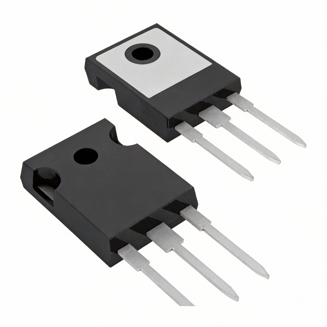 | BSC070N10NS3G | Infineon | 2,820 | |
 | BSC060N10NS3GATMA1 | Infineon | 9,780 | |
 | BSC070N10NS5ATMA1 | Infineon | 7,400 | |
| BSC040N10NS5ATMA1 | Infineon | 4,080 | |
| BSC050N10NS5ATMA1 | Infineon | 8,040 |
It is the typical total gate charge at the datasheet’s stated 50 V bus, 25 A drain current and 0–10 V gate excursion. The corresponding maximum entry is 55 nC. Use those conditions when making an initial driver estimate. Gate charge changes with the operating conditions and is not equivalent to a fixed input capacitance. The value helps estimate drive demand; it does not, by itself, predict converter efficiency or switching time.
The threshold specification does not justify doing so. Threshold is measured at only 75 µA, whereas the 7 mΩ maximum on-resistance is specified with 10 V gate drive at 25°C and a stated drain current. The device also has a different resistance limit at 6 V. A power design needs enough local gate-to-source voltage and transient drive current for its operating point. A logic signal normally needs an appropriately selected gate-drive stage.
Using the simple non-recovering drive model with 42 nC and a 10 V excursion gives 84 mW per MOSFET. Using 55 nC under the same charge-test conditions gives 110 mW. Driver quiescent power and other channels are additional. These estimates describe demand from the gate-drive supply, distributed through the drive circuit and gate resistance. They should not all be assigned to MOSFET junction heating in a thermal calculation.
By Alice Chen
BSC070N10NS3G is Infineon’s 100 V OptiMOS 3 N-channel MOSFET with a 7 mΩ maximum on-resistance at 10 V gate drive. Its 42 nC typical gate charge helps size the driver, but it does not predict converter efficiency by itself. A useful comparison separates conduction, switching overlap and gate-drive power, then checks hot resistance, gate current and commutation conditions. Lower charge pays off only when those surrounding conditions support the change.
This distinction becomes useful when a power stage runs warmer than expected. A quick search may suggest a device with less gate charge, while another offers lower resistance in the same broad package family. Both can be sensible candidates. They address different parts of the loss budget, however, and neither change is automatically an improvement in the existing circuit.
For a hard-switched converter, lower gate charge is most valuable when it reduces a meaningful drive or transition loss without creating a larger conduction, commutation or thermal penalty. For a switch that spends most of its time fully on and changes state infrequently, resistance and heat removal may deserve much more attention. The part’s charge figure becomes useful after the operating role is defined.
Infineon writes the base device as BSC070N10NS3 G and lists the ordering code BSC070N10NS3GATMA1 on its product page. This article retains BSC070N10NS3G as the main model name. It is a normal-level, N-channel device in the SuperSO8, PG-TDSON-8 package family. The datasheet’s pin assignment and exposed drain connection must be checked against the actual PCB library. Similar-looking eight-terminal packages are not sufficient evidence of equivalence. ,
**Figure 1.** Calculated t = Qgd × Rtotal / (Vdrive − Vplateau), using the BSC070N10NS3G typical 7 nC and 4.3 V entries with 10 V drive. Total resistance is an assumed sweep including all gate-path resistance. This simplified turn-on estimate is not measured switching time or a guaranteed waveform. Basis: [Infineon datasheet, p. 4](https://www.infineon.com/assets/row/public/documents/24/49/infineon-bsc070n10ns3-g-datasheet-en.pdf) and [gate-drive application note, pp. 14–18](https://www.infineon.com/assets/row/public/documents/24/42/infineon-gate-drive-for-power-mosfets-in-switchtin-applications-applicationnotes-en.pdf); calculation by YG GROUP. **Figure 2.** Separate calculated power terms for Table 3’s assumptions. The gate-drive curve is supply demand in the drive circuit, not all MOSFET junction heat. Output-capacitance effects, reverse recovery, dead time, driver quiescent power and other converter losses are excluded. This is a sensitivity example, not measured BSC070N10NS3G performance. Device-data basis: [Infineon datasheet, pp. 4–5](https://www.infineon.com/assets/row/public/documents/24/49/infineon-bsc070n10ns3-g-datasheet-en.pdf).A lower-charge device may have different on-resistance, output-charge behavior, diode recovery or interaction with the existing driver. At high current, a conduction penalty can outweigh a modest reduction in gate-drive demand. In other circuits, faster transitions can help substantially but also change overshoot and ringing. Compare the relevant loss mechanisms at the actual voltage, current, duty, frequency and temperature, then verify both efficiency and electrical stress on the board.
No. The datasheet conditions the continuous-current and dissipation ratings on case temperature, and pulse operation remains subject to safe-operating-area limits. A board in ambient air has its own thermal resistance and copper constraints. Rev. 2.2 gives 92 A and 368 A, while the product page still displays 90 A and 360 A; use an identified revision with its conditions. Neither set approves the current capability of an unspecified layout.
No replacement qualification is established here. The product pages verify distinct 100 V base devices and useful resistance, charge and package-family comparisons. They do not establish identical dynamic behavior, full measurement conditions or compatibility with every existing board. Review exact pin assignment, footprint, drive requirements, thermal limits and commutation behavior before substituting. BSC060N10NS3 G is additionally marked not for new design on its product page, so its role here is an existing-design comparison.
The electrical table supplies conditions that a short product description cannot carry. The headline on-resistance belongs to a specified gate voltage and drain current at 25°C. Gate charge belongs to a particular bus voltage, drain current and gate-voltage excursion. These are starting points for analysis, not a complete description of a running converter.
Table 1. BSC070N10NS3G data needed before comparing losses. Values below follow datasheet Rev. 2.2; typical values are identified explicitly. Infineon, pp. 3–5
| Quantity | Published value | Test condition or boundary | How to use it |
|---|---|---|---|
| Drain-source voltage rating | 100 V | Absolute maximum | Check operating voltage and switching overshoot together |
| On-resistance at stronger drive | 6.3 mΩ typical; 7 mΩ maximum | Gate 10 V, drain current 50 A, 25°C | Cold conduction-loss reference |
| On-resistance at lower drive | 8 mΩ typical; 14 mΩ maximum | Gate 6 V, drain current 25 A, 25°C | Demonstrates the cost of a different gate-drive condition |
| Total gate charge | 42 nC typical; 55 nC maximum | Bus 50 V, drain current 25 A, gate excursion 0–10 V | Estimate gate-drive energy at the stated condition |
| Gate-drain charge | 7 nC typical | Same stated charge-test framework | First estimate of the Miller interval |
| Plateau voltage | 4.3 V typical | Datasheet charge characterization | Conditional estimate of available drive current |
| Internal gate resistance | 1.5 Ω typical | Datasheet electrical table | Include with driver and external resistance |
| Junction-to-case resistance | 1.1 K/W maximum | Defined package thermal path | Use with a defensible case-temperature model |
The threshold range is 2.0 to 3.5 V, with a typical value of 2.7 V, measured at only 75 µA. That is a very different condition from carrying converter current with low resistance. It cannot justify driving this device directly from a 3.3 V logic output.
The more useful evidence is the pair of on-resistance specifications. At the stated 10 V condition, the maximum is 7 mΩ. At the stated 6 V condition, it is 14 mΩ. The test currents differ, so this is not a complete matched-current characterization of every operating point. It does show that the low-resistance headline should not follow the part into a lower-drive design without qualification.
A design that relies on the 7 mΩ maximum must preserve the specified gate-drive condition and then account for temperature; the threshold specification does not establish that resistance. Include driver supply tolerance, drops in the gate path and the relevant source reference when checking the actual gate voltage. The value at the controller output is not necessarily the value between the MOSFET’s gate and source terminals.
The manufacturer’s product page lists 90 A continuous and 360 A pulsed, while datasheet Rev. 2.2 specifies 92 A and 368 A under its stated conditions. The revision history explicitly records an update to current ratings. The figures used here follow that identified datasheet revision. Infineon datasheet, pp. 3, 12; product page
Neither pair is a sensible target for an arbitrary board. The continuous rating is conditioned on case temperature, and pulse capability remains subject to the safe operating area and pulse conditions. Treating a current-rating difference as an available design margin would be a distraction from the actual thermal and switching limits.
The first calculation is conduction loss. For a fully enhanced device, the average over a complete cycle is approximately the mean of current squared through the channel, multiplied by the applicable on-resistance. For a simplified rectangular current of amplitude I during duty fraction D, that becomes I² × RDS(on) × D.
The second calculation is switching overlap. During a hard transition, drain voltage and drain current coexist. Their instantaneous product is power; integrating it through the event gives energy. A rough linear-overlap estimate is one half of bus voltage multiplied by switched current and the combined effective overlap time for turn-on and turn-off. Multiplying that energy by switching frequency gives average overlap power.
The third calculation is gate-drive power. A conventional non-recovering gate drive takes approximately Qg × Vdrive × frequency from its supply for each MOSFET. Infineon’s gate-drive application note uses this relationship and explains why the gate current during the plateau depends on drive voltage and resistance. Gate-drive energy is distributed through the drive circuit and gate resistance; it is not automatically all dissipated in the MOSFET die. Infineon gate-drive application note, pp. 14–18
These equations are deliberately separate. If a spreadsheet labels their sum “MOSFET junction heating,” it may put driver dissipation into the wrong thermal model. If it labels the sum “converter loss,” it may omit magnetics, control power, rectification and other substantial terms. The name on the result should match what was actually included.
At a 10 V drive excursion, the typical 42 nC figure corresponds to 420 nJ per switching cycle in the simple gate-drive model. With the published 55 nC maximum at the same charge-test condition, the corresponding energy is 550 nJ. This is a useful range for initial drive-supply planning, provided the actual charge behavior is checked at the application’s voltage and current.
Table 2. Calculated gate-drive demand using the datasheet’s charge entries. These are single-device estimates for a 0–10 V non-recovering drive; driver quiescent power and other channels are excluded. Calculation by YG GROUP using Infineon charge data.
| Switching frequency | Power using 42 nC typical | Power using 55 nC maximum | Average charge current using 42 nC |
|---|---|---|---|
| 50 kHz | 21 mW | 27.5 mW | 2.1 mA |
| 100 kHz | 42 mW | 55 mW | 4.2 mA |
| 200 kHz | 84 mW | 110 mW | 8.4 mA |
| 400 kHz | 168 mW | 220 mW | 16.8 mA |
A small average current in this table does not imply that a weak logic output can drive the device quickly. The charge has to move during a short portion of each cycle. Peak and plateau current can therefore be much larger than the cycle-average current. Confusing the two is an easy way to select a driver that looks adequate in a power budget but produces slow transitions.
The charge table also contains a qualification worth keeping: several capacitance and charge characteristics are defined by design rather than measured in every production test. Preserve the manufacturer’s distinction between a specified maximum, a typical characteristic and the production-test methodology. Do not turn a calculated drive-power column into a promise about every waveform on every unit.
A first approximation to turn-on plateau current is the difference between drive voltage and plateau voltage divided by the total effective resistance in the charging path. That total includes the external resistor, the MOSFET’s internal gate resistance and the driver’s effective source resistance. It is not simply the resistor value printed beside the gate on the schematic.
Using 10 V drive and the 4.3 V typical plateau leaves 5.7 V across that approximate path. With an assumed total resistance of 4 Ω, the estimated current is 1.425 A. Dividing the 7 nC typical gate-drain charge by that current gives a plateau interval of about 4.9 ns. With 8 Ω total resistance, the same simplified estimate becomes about 0.713 A and 9.8 ns.

The estimate assumes representative charge and plateau values, a usable driver voltage, and an effective resistance model. It does not include all current dependence, nonlinear capacitance, parasitic inductance or driver behavior. The datasheet’s gate-charge curves show different bus-voltage conditions; they are a reminder that charge is not one fixed capacitor value multiplied by any chosen voltage. Infineon, p. 9
The model is still useful for asking a focused question: is the intended driver even in the right current range for the desired transition? It is much less useful as a way to claim a precise switching edge before the board exists. Use the result to choose a starting range, then inspect the real drain and gate waveforms under controlled conditions.
Reducing external gate resistance can shorten a transition only while the driver and surrounding circuit support the resulting current and edge rate. A lower resistor can also change ringing, overshoot and susceptibility to unwanted turn-on. The correct value is a compromise tied to the converter’s voltage margin and commutation behavior, not a competition to reach the smallest possible number.
Turn-off deserves its own examination. A driver may have different source and sink characteristics, and the circuit may use different charging and discharging paths. The turn-on calculation in Figure 1 should not be copied into a turn-off timing cell without changing the relevant voltage and resistance assumptions. The off-state gate behavior is particularly important when another device is switching the shared power node.
Consider an illustrative hard-switched position operating from a 48 V bus, with 10 A rectangular channel current during half of each cycle. Use 7 mΩ as the cold resistance input, a 10 V gate drive, the 42 nC typical charge and an assumed combined overlap interval of 20 ns. The overlap interval is an independent assumption. It is not the sum of a few datasheet timing numbers relabeled as a board measurement.
Under those assumptions, conduction loss is 0.35 W. Overlap energy is 4.8 µJ per cycle. Gate-drive energy is 0.42 µJ per cycle. Frequency therefore changes the two dynamic terms while the assumed conduction term stays fixed. This is a sensitivity calculation, not a complete converter design or an efficiency forecast.
Table 3. Calculated power terms for the illustrative 48 V, 10 A scenario. Duty is 0.5, resistance is 7 mΩ, combined effective overlap is 20 ns and gate drive is 10 V with 42 nC typical charge. Calculation by YG GROUP using Infineon electrical data.
| Frequency | Channel conduction | Switching overlap | Gate-drive circuit demand | Interpretation |
|---|---|---|---|---|
| 50 kHz | 0.35 W | 0.24 W | 0.021 W | Conduction is significant in this simplified comparison |
| 100 kHz | 0.35 W | 0.48 W | 0.042 W | Overlap exceeds the cold conduction estimate |
| 200 kHz | 0.35 W | 0.96 W | 0.084 W | Transition behavior deserves close attention |
| 400 kHz | 0.35 W | 1.92 W | 0.168 W | Dynamic terms dominate these selected assumptions |

The example tells an engineer where to look, but only within its assumptions. If the real transition is much slower, overlap loss rises. If the converter switches softly, the hard-overlap model may be inappropriate. If load current rises, conduction changes with current squared while the simple overlap term changes linearly with current. The most important input can therefore change across the operating range.
At 20 A and the same assumed duty, the cold conduction calculation becomes 1.4 W. If a separate thermal sensitivity case uses 14 mΩ as an assumed hot resistance, it becomes 2.8 W. That second resistance is an explicit example input; it is not a guaranteed hot value at a named temperature taken from the typical curve. The exercise demonstrates why a room-temperature comparison can understate the importance of thermal operation.
The same example can identify where the selected conduction and overlap terms become equal. Dividing 0.35 W by 4.8 µJ gives approximately 73 kHz. Above that frequency, the assumed overlap term exceeds the cold conduction term. This is not an optimum operating frequency for BSC070N10NS3G. It is a breakpoint inside one deliberately simplified model.
At a rectangular current of 20 A, with the same duty, resistance and assumed transition duration, conduction becomes 1.4 W and overlap energy becomes 9.6 µJ. The corresponding crossover is about 146 kHz. Doubling current has moved the balance because conduction increased fourfold while the simplified overlap energy doubled. That is a concrete reason to compare devices at both light and heavy load rather than only at one convenient operating point.
The assumed transition duration is the vulnerable input in both calculations. In a real converter, changing current can change the plateau, driver interaction and commutation behavior. If measurement shows that the interval is not constant, update the model before using its crossover to justify a component change. A sensitivity calculation is most useful when it makes the missing evidence easy to identify.
For example, if a design operates well below the model’s crossover at its important load point, first investigate hot resistance and the thermal path. If it operates far above it, a properly measured transition-energy comparison may provide more useful information than another cold resistance measurement. This is a way to allocate engineering effort, not a rule that excludes the smaller term.
Do the comparison at the product’s important operating points, too. A converter that spends most of its life at a light load can favor a different compromise from one that operates continuously near its maximum output. The mission profile is an input to selection. It should not be replaced by whichever laboratory condition makes a preferred device look best.
The datasheet lists nonlinear output capacitance and output charge, as well as body-diode recovery characteristics. These point to additional switching behavior that the simple overlap model omits. The 520 pF typical output-capacitance entry belongs to its stated bias and frequency. It should not be treated as a voltage-independent capacitor across the entire switching excursion. Infineon, pp. 4–5, 8
Reverse recovery has its own conditions. The typical 112 nC recovery charge is specified at a reverse voltage of 50 V, forward current of 25 A and current slew rate of 100 A/µs. A different commutation event can behave differently. It is not defensible to multiply that one value by an unrelated bus voltage, append the result to the table and present the sum as a guaranteed device loss.
Instead, keep excluded mechanisms visible. If dead-time diode conduction is material, analyze it for the actual dead time and current. If output-charge energy is important, use an appropriate voltage-dependent model or validated device data. A clearly incomplete first estimate is easier to improve than a supposedly complete answer whose extra percentage margin hides several unrelated effects.
The following shortlist stays within 100 V N-channel devices with the SuperSO8 package family. That makes the comparison relevant, but it does not make it complete. The manufacturer’s product pages provide the resistance, typical charge and ordering identities shown here. The charge entries are labeled at 10 V, while the pages do not expose every bus-voltage and current condition needed for a rigorously matched comparison. [4–7]
Table 4. Four distinct related base devices for further evaluation. Resistance is the product-page maximum at 10 V gate drive; charge is the product-page typical value at 10 V. These are screening fields, not an approved substitution matrix.
| Exact ordering MPN | Verified base device | On-resistance maximum | Gate charge typical | Useful comparison and boundary |
|---|---|---|---|---|
| BSC060N10NS3GATMA1 | BSC060N10NS3 G | 6 mΩ | 51 nC | Nearby OptiMOS 3 tradeoff; page marks it not for new design |
| BSC070N10NS5ATMA1 | BSC070N10NS5 | 7 mΩ | 30 nC | Similar headline resistance with lower typical charge; technology and dynamics need review |
| BSC040N10NS5ATMA1 | BSC040N10NS5 | 4 mΩ | 58 nC | Lower headline resistance with a larger charge figure |
| BSC050N10NS5ATMA1 | BSC050N10NS5 | 5 mΩ | 49 nC | Intermediate resistance and charge within this shortlist |
The difference between 42 nC and 30 nC gives a simple way to judge scale. At 10 V and 200 kHz, a hypothetical reduction of 12 nC lowers conventional gate-drive demand by 24 mW. That is a calculation using the displayed charge difference, not a measured benefit of replacing one device with another. It says nothing by itself about overlap energy, which may change by a different amount.
Now compare a hypothetical resistance reduction from 7 to 4 mΩ at 10 A and duty 0.5. The cold conduction saving is 0.15 W. A charge increase from 42 to 58 nC adds 32 mW to the simple gate-drive estimate at the same 10 V and 200 kHz. Under these selected inputs, the conduction term is larger. At a lighter load or a different frequency, the balance changes.
This is why an on-resistance-times-charge figure of merit is a useful sorting aid rather than a complete verdict. It compresses two attributes but leaves out topology, thermal paths, output charge, recovery and the driver’s interaction with the device. A part can rank well by that product and still be the wrong choice for a particular switching position.
The lower-charge NS5 device is a credible candidate when dynamic behavior limits the design, but its product-page figures do not prove a drop-in efficiency improvement. Check the full electrical conditions, footprint, pin assignment, thermal capability and operating waveforms before approving a substitution. The NS3 neighbor marked not for new design is best treated as a comparison for an existing design, not an unqualified recommendation for a new platform.
The 114 W dissipation rating is specified at a case temperature of 25°C. It does not mean a small PCB can dissipate 114 W into ordinary room air. Maintaining that case temperature requires a thermal environment that the number itself does not provide. The junction-to-case value and a board’s junction-to-ambient behavior answer different questions. Infineon, p. 3
The datasheet gives junction-to-ambient examples tied to mounting conditions, including 50 K/W with a defined copper area and board construction. Even applying that value to the earlier 1.4 W conduction example would imply a 70°C junction-to-ambient rise before additional losses were included. That arithmetic is a warning about the scale of the thermal problem, not a prediction for a different layout.
A defensible thermal model identifies where temperature is known or measured and which thermal path connects that point to the junction. It then uses losses appropriate to the hot operating state. Otherwise, the calculation can become circular: cold resistance predicts modest heating, while the actual hotter device has more resistance and greater dissipation.
Transient operation needs similar care. The safe operating area and transient thermal impedance curves are conditioned on pulse duration and thermal state. A large pulsed-current number cannot approve a long linear-mode interval during startup or a fault. If the application asks the device to support voltage and current together for an extended interval, review that operating point directly against the relevant evidence.
A useful bench comparison preserves the conditions that matter: bus voltage, load, switching frequency, driver supply, gate resistor, temperature and measurement setup. Changing several at once may improve the converter, but it makes the contribution of the MOSFET difficult to identify. Start with the loss mechanism that the calculation says is likely to dominate.
Table 5. Match a design concern to a measurement or review. YG GROUP editorial validation sequence, informed by Infineon device characteristics; these tests have not been performed for this article.
| Concern | Evidence to collect | Decision it informs |
|---|---|---|
| Insufficient gate enhancement | Gate-to-source voltage at the device under operating conditions | Drive supply and resistance selection |
| Excessive transition loss | Time-aligned drain voltage and current with probe effects understood | Driver, gate path and switching-device choice |
| Ringing or voltage overshoot | Local gate and drain waveforms at relevant loads | Gate resistance, layout and voltage margin |
| Unexpected heating | Defined temperature measurement and thermal-path model | Copper, cooling and hot-loss assumptions |
| Commutation behavior | Dead-time and diode-related waveforms in the actual topology | Timing and device-family comparison |
| Proposed replacement | Exact package review plus repeated relevant electrical checks | Qualification of the alternative in that design |
When calculating switching energy from voltage and current traces, timing alignment matters. A small relative delay between probes can create or hide an apparent overlap area. Document the probing arrangement and compensation method before treating the integral as an accurate loss measurement. A clean-looking waveform is not a substitute for knowing how it was acquired.
The same caution applies to measuring gate voltage. A distant ground connection may include source movement that is not present in the way assumed by the gate-drive calculation. The relevant voltage is local gate-to-source voltage, especially during fast transitions. The layout around the driver and source return therefore belongs in the interpretation of the trace.
After a component change, repeat the checks that could invalidate the apparent benefit. Reduced input power is encouraging, but the device may have gained ringing or lost voltage margin. Lower case temperature is useful, but a different heat path can complicate a direct comparison. Accept the improvement only when efficiency, stress and thermal behavior tell a consistent story at the operating points the product actually uses.
BSC070N10NS3G provides enough information to make a disciplined first calculation: separate gate-drive demand, channel conduction and switching overlap; preserve each parameter’s test conditions; and keep the omitted mechanisms visible. The result should direct a measurement or a design choice, not pretend to replace either one.
Lower charge is attractive when frequency and transition behavior make dynamic losses important. Lower resistance becomes more valuable as current and conduction duty grow. The useful device is the one that achieves the required balance with the available gate driver, cooling and voltage margin. That judgment is more reliable than picking the smallest charge number from a list of similar packages.