
YG Group



3 views

| Picture | Part Number | Manufacturer | Stock | Action |
|---|---|---|---|---|
 | 74ALVCH32973ZKER | Texas Instruments | 4,330 |
No. The documented function is a 16-bit transceiver and 16-bit transparent latch with eight independent noninverting buffers. The transceiver and latch are different roles associated with the bus; their widths should not be added to invent a 32-bit latch. Use the function diagrams and exact ordering information rather than decoding channel count from the digits in the name.
The supplied ordering appendix is dated March 30, 2005. Its status describes that historical document. TI PDN20191218000.3, dated January 7, 2020, is later evidence covering the exact order, with last-order and last-shipment dates of January 7 and July 7, 2021. This is a chronology issue, not evidence of a newly announced EOL in 2026.
No drop-in conclusion is established here. TI identifies it as a functional candidate, but one device has an 8-bit transceiver/latch and four buffers. Matching the original functional counts with two devices still leaves package, control, timing, electrical and layout qualification. Use the candidate as a redesign starting point rather than a purchase-order substitution.
Author: YG Group | Primary part: 74ALVCH32973ZKER | Manufacturer: Texas Instruments
74ALVCH32973ZKER is a Texas Instruments bus-interface device combining a 16-bit transceiver and transparent latch with eight independent buffers. Its 96-ball LFBGA package and 1.65V to 3.6V operating range support legacy address/data-bus demultiplexing. TI's historical discontinuance notice makes redesign planning relevant, but a listed functional candidate is not a drop-in substitute: channel count, control behavior, bus hold, timing and board layout still require verification.
The redesign starts by separating the functions hidden inside the original package. Establish which signals need bidirectional transfer, which need transparent address capture and which simply pass through independent buffers. Only then can a candidate list become a meaningful engineering decision.
Read the identity and lifecycle chronology, , , , , or .
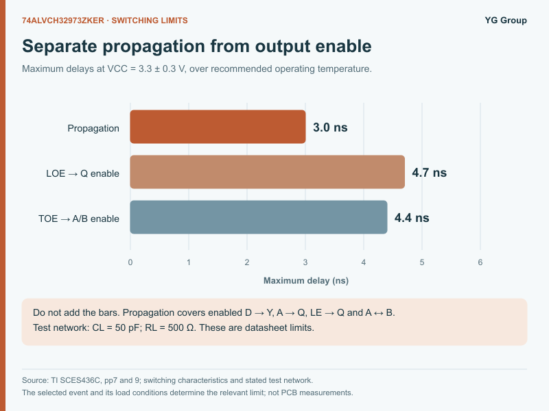
*Figure 1: Original transceiver, transparent-latch and independent-buffer roles | Source: [TI SCES436C, pp1–4, public document mirror](https://datasheet.lcsc.com/datasheet/pdf/94e3f24b13554afeb66318fe48ca3466.pdf?productCode=C122836) | Chart: YG Group* *Figure 2: Propagation and enable maxima are separate timing terms | Source: [TI SCES436C, pp7 and 9, public document mirror](https://datasheet.lcsc.com/datasheet/pdf/94e3f24b13554afeb66318fe48ca3466.pdf?productCode=C122836) | Chart: YG Group*No. Bus hold applies to specified data nodes, while unused controls and startup output enables require separate treatment. TI specifically distinguishes those requirements. Identify the node's role before adding or removing a resistor; an indiscriminate pull network can conflict with the intended bus-hold behavior or fail to establish the required startup control state.
The recommended supply range is 1.65–3.6 V. The 4.6 V entry is an absolute-maximum stress boundary, not a normal operating point. Input and output limits must also be checked separately; the supply stress rating does not make every connected pin tolerant of that voltage during operation.
No. Under the stated 3.3 V ±0.3 V test conditions, 3 ns is the listed maximum propagation delay for the specified paths. Output-enable timing, disable timing, latch setup, hold and pulse-width requirements are separate. A board-level timing budget must select the appropriate parameter for its actual event and retain the relevant supply, temperature and loading conditions.
Use the complete 74ALVCH32973ZKER order code for the lifecycle conclusion. The supplied TI datasheet and a later TI discontinuance notice answer different questions, so an old Active entry cannot overturn the later exact-part event.
The technical baseline is TI SCES436C, revised September 2004. Its first-page ordering table identifies the Pb-free ZKE option as 74ALVCH32973ZKER, without an added SN prefix, and the supplied March 30, 2005 package addendum lists the 96-ball LFBGA. Family headings use SN74ALVCH32973; that heading does not authorize changing the purchase order's spelling. A public mirror of the TI-authored Rev. C datasheet makes the technical pages available for reference; its later appended material must not be confused with the supplied 2005 appendix.
| Evidence date | Document or event | Exact-device meaning | How to use it |
|---|---|---|---|
| September 2004 | SCES436C technical revision | Defines the multifunction logic and electrical behavior | Baseline the functions and operating conditions |
| March 30, 2005 | Supplied package addendum | Lists 74ALVCH32973ZKER, 96-ball ZKE and historical Active status | Establish historical ordering identity, not present lifecycle |
| January 7, 2020 | TI PDN20191218000.3 | Includes the exact order and a functional candidate | Establish the later discontinuance record |
| January 7, 2021 | Notice's last-order date | Historical manufacturer ordering deadline | Do not present it as a new deadline this week |
| July 7, 2021 | Notice's last-shipment date | Historical manufacturer shipment deadline | Do not infer all downstream inventory disappeared then |
| September 10, 2026 | Source article's evidence check | Reconciles the supplied document with the later notice | Keep current seller availability as a separate question |
Table 1: Exact-device identity and historical discontinuance chronology | Source: TI PDN20191218000.3 and TI SCES436C technical document mirror | Compiled by: YG Group
The practical implication is to maintain two records. The engineering record holds the original part identity, document versions and candidate qualification. The sourcing record holds dated offers for the exact part, quantities, packaging and any required traceability. Neither record can substitute for the other: EOL is not proof of zero remaining stock, and a current offer is not proof that a new design should retain the discontinued component.
Before redesigning, also verify that the installed assembly really uses this order. An old schematic may contain only the family name, while the bill of materials, approved-source list and package drawing contain more specific information. Resolve those records together. If they disagree, do not make the new footprint from the shortest label in the archive.
The objective is not to turn a 2020 notice into fresh market news. It is to use that notice as the reason for a present engineering task: maintaining a legacy product without assuming that a similarly named logic device will preserve its behavior. The useful output is a controlled redesign specification that can survive a change of component and a change of engineer.
The original device contains three functional roles with different control dependencies. Preserve those roles explicitly, because replacing one of them does not automatically replace the others.
The A and B buses form a bidirectional transceiver path. Direction control chooses which bus drives the other, while the transceiver output-enable control can isolate that path. Separately, the latch captures information from A onto Q. When latch enable is high, the enabled Q outputs follow A; when latch enable goes low, the captured state is retained. The latch output-enable control changes whether Q drives externally, not whether the internal latch can retain or accept data. These distinctions come from the TI function tables and logic diagrams, pp1–4.
| Functional block | Channel count | Data path | Relevant controls | Behavior to preserve |
|---|---|---|---|---|
| Bidirectional transceiver | 16 bits, organized in two groups | A to B or B to A | Group DIR and TOE | Direction, isolation and handover between bus owners |
| Transparent latch | 16 bits, organized in two groups | A to Q | Group LE and LOE | Transparent interval, closing event and independent output enable |
| Independent noninverting buffers | 8 | D to Y | Independent of DIR, TOE, LE and LOE | Y follows D without borrowing a latch/transceiver enable |
Table 2: Functional decomposition of the original bus-interface device | Source: TI SCES436C, pp1–4, public document mirror | Compiled by: YG Group
A common redesign error is to model the latch as an edge-triggered register. The falling edge of LE closes a transparent interval; it does not make the interval before that edge irrelevant. If the receiving circuitry observes Q while the latch is transparent, changes on A can matter before capture. A register-based redesign might be valid, but only after the system's observation and timing requirements have been changed or shown to be compatible.
Another error is to assume one output-enable signal controls the entire package. The eight D-to-Y buffers are independent of the four named latch/transceiver controls. As a result, disabling the A/B path and Q outputs does not, by itself, establish an all-package high-impedance state. Identify where each Y output goes and whether its receiving circuit requires an additional system-level startup condition.
Build a net-role inventory from the old schematic. For every used signal, record the source, destination, direction, active phase and required inactive state. Mark whether the signal must remain available while the transceiver is isolated. Mark unused data nodes separately from unused control inputs. This inventory catches dependencies that a simple pin-count comparison cannot reveal.
Use changing patterns rather than only all-zero and all-one words when checking the inventory. A single asserted bit moving across the word can reveal crossed channels; alternating patterns exercise adjacent signal relationships; separate patterns on the two eight-bit groups reveal accidental coupling of their controls. For the latch, change A while LE is high, close LE, and then change A again. Observe Q with its output enabled and repeat while it is disabled, verifying the retained state when the output returns. These are proposed functional tests derived from the documented truth table, not measurements of a completed replacement.
Consider a hypothetical 16-bit multiplexed controller interface. During its address phase, the controller presents an address on A, LE allows the address to pass to Q, and the closing event retains it for the later data phase. During a read, another device may drive B toward A; during a write, A may drive B. Eight separate D-to-Y paths carry unrelated control signals. This example describes a possible use of the documented functions, not a recovered customer schematic or a validated replacement circuit.
To qualify a split implementation, walk that sequence with the proposed controls. Ask whether address capture still occurs while the relevant data are stable, whether changing direction exposes contention, and whether independently buffered controls arrive in the intended phase. A two-chip or three-chip solution can match the Boolean roles yet alter the relative arrival times enough to require a new timing budget.
Review the 16-bit A↔B path, the 16-bit A→Q transparent-latch path and eight D→Y buffers as distinct functions. The two control groups must retain their separate behavior; a single global enable cannot describe the original interface. Matching this functional structure is necessary, but it does not by itself establish a complete replacement pinout or schematic.

An interface migration can require board and behavior changes even when the new part has a nominally similar role. This concern applies across interface types, but another interface's specifications cannot qualify the parallel-bus logic here. Identify each required function, its control dependencies and the surrounding circuit before judging a candidate.
Bus hold and safe control states solve different problems. The original device provides bus-hold circuitry on the A and B I/Os and D inputs, while unused control inputs and startup output enables require their own defined treatment.
TI advises against adding pullup or pulldown resistors to the bus-held data inputs as a default remedy. It separately directs the designer to pull LOE and TOE toward VCC to establish the stated high-impedance behavior during power-up or power-down, with resistor selection constrained by the controlling drivers' sinking capability. Those statements are compatible: they concern different nodes and different purposes. SCES436C, p1 and p5 note 1.
| Requirement | Documented boundary | Node or condition | Redesign implication |
|---|---|---|---|
| Recommended supply | 1.65–3.6 V | VCC | Select an operating voltage, not the 4.6 V stress limit |
| Normal input/output range | 0 to VCC | Recommended operation | Check each connected device's levels separately |
| High/low input thresholds at 3–3.6 V VCC | VIH minimum 2 V; VIL maximum 0.8 V | Applicable supply band | Compare guaranteed driver output levels at the actual load |
| Output-current operating entries | ±24 mA at VCC = 3 V; ±4 mA at VCC = 1.65 V | Per documented output-current conditions | Do not carry the 3 V drive number into a 1.65 V design |
| Data bus hold | A/B I/Os and D inputs | Undriven data nodes | Review candidate hold behavior and avoid indiscriminate pulls |
| Startup output enables | LOE and TOE pulled toward VCC | Transceiver and latch output paths | Check controlling driver, sequencing and resistor loading |
| Unused control inputs | Held at VCC or GND | Control pins | Do not leave them floating because data nodes have bus hold |
Table 3: Electrical and startup conditions that survive a package change | Source: TI SCES436C, pp1, 5–6, public document mirror | Compiled by: YG Group
A useful startup review follows the power domains rather than the nominal logic diagram. Identify which device drives each control while reset is asserted, while one rail is present and another is absent, and while the controller changes a pin from its reset function to its operating function. Do not assume a replacement's powered-off behavior matches the original simply because its operating supply range overlaps.
For the resistor decision, begin with the required inactive logic level, the candidate's leakage and the controller's guaranteed sink capability. Then check the transition time and the current when the control is asserted. This article does not select a universal pullup value because the driver, capacitance and startup timing have not been supplied. A resistor value copied from an unrelated board would create apparent specificity without establishing a valid design.
Observe startup at the pins that matter to the receiving circuit. Measuring a clean control signal at the controller is not the same as proving the enabled output remains harmless at the load. Check the intended inactive state, the first driven transition and any overlap between opposing bus drivers. Include power-down and reset recovery, not only a normal cold start.
Logic defaults need explicit review whenever a component changes. Behavior documented for an isolated interface does not establish the default state of this parallel-bus device. Make the required startup and inactive states part of the replacement specification, then verify them against the candidate and board instead of assuming they follow from a replacement label.
Use the timing parameter for the event being analyzed. Propagation through an already enabled path, enabling a previously isolated output and closing a transparent latch are different events, even when they occur in the same bus cycle.
TI's 3.3 V ±0.3 V column gives the values below over the recommended operating free-air temperature range, unless otherwise noted. The associated measurement network uses 50 pF and 500 Ω as specified on p9. That laboratory load definition is part of the specification; it is not a model of every PCB or receiving device.
| Event or path | Parameter type | Relevant limit | Supply/test condition | What the value does not establish |
|---|---|---|---|---|
| Enabled D→Y, A→Q, LE→Q or A↔B propagation | Maximum propagation delay | 3.0 ns | 3.3 V ±0.3 V; specified 50 pF/500 Ω network | Every output-enable or board-level path |
| LOE→Q output enable | Maximum enable delay | 4.7 ns | Same supply and measurement scope | Latch setup or data propagation after a later change |
| TOE→A/B output enable | Maximum enable delay | 4.4 ns | Same supply and measurement scope | Complete bus-turnaround margin |
| Data before LE falls | Minimum setup time | 0.9 ns | Timing-requirements table, same supply column | Required downstream receiver setup |
| Data after LE falls | Minimum hold time | 0.9 ns | Timing-requirements table, same supply column | Minimum delay of an added external data path |
| LE high interval | Minimum pulse duration | 2.0 ns | Timing-requirements table | A safe clock frequency for an unspecified system |
Table 4: Distinct timing requirements under the stated TI conditions | Source: TI SCES436C, pp7 and 9, public document mirror | Compiled by: YG Group
Consider an illustrative enabled data path with 8 ns available from a source transition to a receiver's capture event. Assume the original logic's applicable maximum delay is 3 ns, routing and other board delay are budgeted at 1 ns, and the receiving device requires 1 ns setup. The arithmetic margin is 8 − 3 − 1 − 1 = 3 ns. Only the 3 ns logic term comes from Table 4; the other quantities are explicit example assumptions requiring real design evidence.
If the event instead begins by enabling the Q outputs, substituting the relevant 4.7 ns LOE-to-Q term into that illustrative budget leaves 1.3 ns. Do not add 3 ns and 4.7 ns automatically: whether separate delays accumulate depends on the actual causal path and timing definition. Conversely, do not use the smaller propagation number for an enable event merely to obtain a positive margin.
Hold-time analysis needs its own minimum-delay path. A design can satisfy the maximum-delay setup budget and still change data too soon after capture. For a split implementation, compare the earliest possible new data arrival with the latest relevant capture/control event, including skew. The minimum hold requirement is not an extra maximum propagation delay to add to a setup equation.
Bus turnaround is another distinct check. Establish when the old driver stops driving and when the new driver can begin. Compare the appropriate disable and enable limits, controller sequencing and route differences. A nominal software delay or a typical waveform does not prove absence of contention across the specified conditions. Likewise, an excessively long high-impedance gap can affect the receiving logic's interpretation even if contention is avoided.
Under the stated common supply, load network and temperature conditions, the maximum delays are 3.0 ns for propagation, 4.7 ns for LOE-to-Q enable and 4.4 ns for TOE-to-bus enable. These values describe different initiating events. Choose the term that matches the actual transition being budgeted; adding all three would not produce a meaningful universal delay for the device.
Protection and loading outside the replacement IC remain board-level questions. Interface components, traces and receiving loads can affect the behavior observed at the system boundary. Include their effects in the actual design instead of expecting a logic timing table to qualify the complete interface; use the relevant specifications for each external element.
The TI notice identifies SN74ALVCH16973DGGR as a functional candidate, but one candidate device does not reproduce the original channel count. The candidate combines an 8-bit transceiver/latch with four buffers; two devices are needed to cover the original 16-bit and eight-buffer counts before considering package, control and timing details.
TI's logic support discussion of this migration also describes using two SN74ALVCH16973 devices for the functional roles. That support answer is useful architectural guidance, not a released schematic or proof of pin compatibility. Candidate electrical limits must still come from each candidate's own documentation.
| Model | Relationship | Function available | Important gap to qualify |
|---|---|---|---|
| 74ALVCH32973ZKER | Primary baseline | 16-bit transceiver/latch plus eight buffers | Discontinued exact device; baseline for the review |
| SN74ALVCH16973DGGR | Potential alternative; TI functional candidate | 8-bit transceiver/latch plus four buffers | Half the functional width per device; new package/layout and timing review |
| SN74ALVCH16245DGGR | Comparison candidate | 16-bit transceiver block | Does not supply the latch or independent-buffer functions |
| SN74ALVCH16373DGGR | Comparison candidate | 16-bit transparent-latch block | Does not supply bidirectional data transfer |
| SN74LVC244APWR | Comparison candidate | Eight-buffer block | Different enable organization and bus-hold/electrical behavior need review |
Table 5: Function-related candidates, not an approved drop-in list | Source: TI SN74ALVCH16973, SN74ALVCH16245, SN74ALVCH16373 and SN74LVC244A documentation | Compiled by: YG Group
A split design changes more than placement area. It can add control fanout, route length, relative skew and separate decoupling locations. Review whether shared control signals still reach both halves with acceptable timing and whether their inactive states remain defined. Keep power-domain behavior, footprint and assembly constraints in the same change record as the logic comparison.
Compare two implementation strategies on the same requirements sheet. A pair of multifunction candidates may retain a recognizable grouping of controls, while separate transceiver, latch and buffer devices may offer more placement flexibility. Neither approach is automatically smaller, faster or easier to qualify. Count the actual required functions, control connections and power pins, then estimate board impact from the selected packages. If only part of the original device was used, document that reduced requirement rather than designing every candidate around unused channels.
Before approving samples, produce a pin-role mapping, a candidate-by-candidate limits comparison and a test plan covering startup, normal transfers, latch closure and bus turnaround. Define the acceptance limits before looking at measurements. Otherwise, a waveform that looks plausible can become the standard simply because it is the first result obtained.
Keep the evidence associated with each board revision. A timing result from an early prototype does not automatically qualify a later reroute, a different pullup or a changed receiving load. Record the supply settings, observation points and instrument loading with the test, then repeat the affected checks when those conditions change. This makes the qualification reusable without pretending that one successful capture establishes every future configuration.
Separate controller logic from the electrical interface when planning a redesign. A system protocol, the logic that controls data flow and the circuitry that drives the physical connection each need their own evidence. Devices intended for a different interface are not substitutes for this bus component simply because they serve a broad communication role.
For an existing-product maintenance decision, check current availability of the exact 74ALVCH32973ZKER order or a separately qualified candidate. Include the complete manufacturer/model identity, quantity and required packaging in a quotation inquiry. Historical EOL does not prove that no stock remains, and a present offer does not qualify a replacement's electrical or functional behavior.
The defensible redesign is the one that preserves the required functions and timing, not the one with the closest part number. Keep the historical TI notice, map the transceiver, latch and buffer roles, define startup controls, and rebuild each timing path with the actual candidate and load. That process turns an EOL response into an engineering release decision with explicit evidence and limits.