
Georgia Huang




| Picture | Part Number | Manufacturer | Stock | Action |
|---|---|---|---|---|
 | XC5VLX155T-1FFG1738I | Xilinx | 3,550 | |
 | XC5VLX155T-1FFG1136I | Xilinx | 2,280 | |
 | XC5VLX330T-1FFG1738I | Xilinx | 1,210 |
The maximum is 680 user I/Os in the FFG1738 package, according to Table 2 of Xilinx DS100 v5.1. The same LX155T device in FFG1136 exposes 640. The 680 figure excludes GTP transceivers and is not a guarantee that every remaining connection can serve any interface. Bank supplies, electrical standards, differential pairing, clock access, and the exact pin assignment determine whether your required interfaces can coexist. Use the package-specific pinout when making the board assignment.
No. DS100 v5.1 lists 16 GTP transceivers for both LX155T package combinations. FFG1738 increases maximum user I/O from 640 to 680 and increases the package body from 35 × 35 mm to 42.5 × 42.5 mm. It does not increase the die's slices, DSP48E resources, or block RAM. If serial-lane count is the limiting resource, investigate a device with more lanes rather than assuming that this package change supplies them.
In the DS100 ordering diagram, I identifies the industrial junction-temperature range of −40°C to +100°C. Junction temperature describes the silicon, not the surrounding air. The permitted ambient condition depends on actual dissipation, board construction, package thermal behavior, and cooling. The -1 field is a separate speed grade. Neither suffix provides a single guaranteed frequency for every user design; use the detailed electrical specifications and implemented timing reports for the intended conditions.
Author: Georgia Huang
Category: 芯片选型与替代 / FPGA与自适应SoC选型
XC5VLX155T-1FFG1738I is a Virtex-5 LXT FPGA with 24,320 slices, 212 blocks of 36-Kbit block RAM, and 16 GTP transceivers. Its FFG1738 package exposes a maximum of 680 user I/Os. That combination makes package selection a separate engineering decision from logic capacity: the smaller FFG1136 version of the same FPGA has the same transceiver count but only 640 user I/Os. Start with the interfaces your board must carry, then decide which package earns its footprint.
A resource summary can make this device look straightforward. Count the logic, count the pins, leave a margin, and move on. The harder question is whether the remaining resources can serve the particular interfaces in your design. A spare pin in the wrong bank does not help a bus that needs a different bank supply. A spare transceiver does not fix a reference clock routed to the wrong place. Empty logic cannot replace an unavailable package connection.
For an existing acquisition or communications board, the attraction of this FPGA is the combination of substantial programmable logic, internal buffering, parallel I/O, and dedicated serial connectivity. Those resources can keep framing, buffering, and interface control close together. They also create several different resource limits. A design may be modest in slice usage and still be difficult to place because its interface locations leave little freedom.
The FFG1738 package should be justified by an actual pin and bank assignment, not by the apparent comfort of a larger ball count. This is an engineering recommendation based on the package and resource distinctions in Xilinx's , particularly Tables 1 and 2. It is not a claim that the smaller package is always preferable. On a board that needs the additional connections, the larger package may be the more practical starting point.
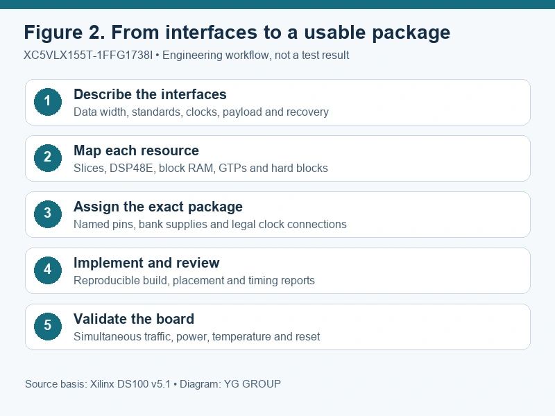
*Figure 1. Package exposure and device growth are different choices. LX155T moves from 640 to 680 user I/Os when changing from FFG1136 to FFG1738, while retaining 16 GTPs. LX220T in FFG1738 also has 680 I/Os and 16 GTPs; LX330T in that package has 960 I/Os and 24 GTPs. Source: [DS100 v5.1](https://docs.amd.com/v/u/en-US/ds100), Table 2. Chart: YG GROUP.* *Figure 2. A package decision becomes credible when resource mapping and pin assignment lead to a reproducible implementation and a board validation plan. This is an engineering workflow, not a measured test result. Source basis: [DS100](https://docs.amd.com/v/u/en-US/ds100), with the pinout and timing document roles described on p. 15. Diagram: YG GROUP.*It is a useful comparison when programmable logic is the bottleneck. DS100 lists 34,560 slices for LX220T versus 24,320 for LX155T. However, both list 128 DSP48E slices, 212 blocks of 36-Kbit RAM, 16 GTPs, and 680 user I/Os in FFG1738. A move to LX220T therefore does not solve every resource shortage. Pinout, power, configuration, implementation, timing, and thermal behavior still require review. This comparison does not approve a drop-in replacement.
Only as an early capacity estimate. LX155T contains 212 blocks of 36-Kbit RAM, with supported configurations and optional FIFO functions described in DS100. Actual resource use depends on queue width, depth, port requirements, latency, and placement. Interface logic can consume block RAM too. Several independent shallow buffers may map differently from one large buffer with the same total payload. Review the mapped implementation rather than treating the published bit total as freely interchangeable storage.
That is not what this notice establishes. XCN12011 concerns particular revision-control SCD ordering codes and identifies standard replacements. It provides historical evidence for the standard ordering codes listed in its tables. The notice alone does not establish the current lifecycle, stock, or lead time of XC5VLX155T-1FFG1738I. Check those commercial facts separately against current manufacturer and supplier information. Technical selection and current availability are different questions, even when they appear in the same procurement discussion.
Before comparing prices or changing a bill of materials, separate three questions. Does the device contain enough of each resource? Does the package expose the connections needed by the board? Can those connections satisfy the electrical and timing requirements together? Answering the first question alone leaves the most expensive board decisions unresolved.
The LX155T device belongs to the LXT platform. The T matters: this is the branch with GTP serial connectivity. The speed grade is -1, the package is FFG1738, and the final I denotes the industrial junction-temperature range. These are independent selection fields. A spreadsheet that keeps only XC5VLX155T has dropped information required to reproduce the original selection.
Table 1. Identity and resources that matter to the board decision
| Item | XC5VLX155T-1FFG1738I | Practical meaning |
|---|---|---|
| Platform and device | Virtex-5 LXT, XC5VLX155T | General logic combined with GTP serial connectivity |
| Logic slices | 24,320 | Check mapped slice usage and placement, not a different family's logic-cell label |
| DSP48E slices | 128 | Dedicated arithmetic resources need their own allocation |
| Block RAM | 212 × 36 Kbit; 7,632 Kbit total | Memory shape, ports, and placement can constrain usable buffering |
| GTP transceivers | 16 | Separate resources from general-purpose user I/O |
| Maximum user I/O in this package | 680 | Upper package count before design-specific assignment constraints |
| Package | FFG1738, 42.5 × 42.5 mm | Mechanical body dimensions; not PCB courtyard dimensions |
| Speed and temperature suffix | -1; I = −40°C to +100°C junction | Timing and thermal qualification must use the selected grade |
Source: Xilinx DS100 v5.1, August 21, 2015, pp. 2, 11–12. Compiled by YG GROUP. Original documentation.
DS100 distinguishes G packaging from V packaging in its ordering diagram. It identifies G as RoHS 6/6 with exemption 15 and V as RoHS 6/6. The package table also limits which V combinations exist. That historical nomenclature is useful for interpreting the code; it does not replace current material declarations or establish compliance for a particular received lot. Preserve the full ordering code when requesting documentation.
The industrial range in the table is a junction-temperature range, not a guarantee that the surrounding air can reach +100°C while the FPGA dissipates arbitrary power. A thermal calculation needs the actual board, cooling, activity, and package data. Likewise, -1 is a timing grade rather than a single operating-frequency specification. Different paths, clocks, I/O standards, and hard blocks have different timing requirements.
The most revealing comparison keeps the FPGA die constant. In DS100 Table 2, XC5VLX155T is offered with FFG1136 and FFG1738. The smaller package lists 640 user I/Os and 16 GTPs. The larger lists 680 user I/Os and the same 16 GTPs. The difference is forty user I/Os, not an increase in programmable logic or serial lanes.
Table 2. Same LX155T device, different package exposure
| Comparison | FFG1136 | FFG1738 | Selection implication |
|---|---|---|---|
| Package body | 35 × 35 mm | 42.5 × 42.5 mm | Recheck board space and mechanical clearance |
| Maximum user I/O | 640 | 680 | Larger package adds 40 general-purpose connections |
| GTP transceivers | 16 | 16 | No serial-lane increase from this package change |
| Logic slices | 24,320 | 24,320 | Same device-level logic capacity |
| 36-Kbit block RAM blocks | 212 | 212 | Same device-level block-memory capacity |
| Calculated package body area | 1,225 mm² | 1,806.25 mm² | About 47.4% more body area, excluding courtyard and routing |
Source: DS100 v5.1, Tables 1–2. Areas are YG GROUP calculations from the stated body dimensions, not board-area measurements.
The arithmetic is useful because it stops two different advantages from being mixed together. FFG1738 gives 6.25% more maximum user I/O than FFG1136, while its rectangular body area is about 47.4% larger. Neither percentage predicts assembly cost, routing effort, or complete board size. Escape routing and power distribution can dominate those outcomes. They do show why the package deserves an explicit reason in the design review.

Consider a board whose parallel interfaces already require most of the smaller package's exposed connections. Forty extra I/Os could avoid external multiplexing, a narrower interface, or a second programmable device. In that situation, the larger body can simplify the system even though it occupies more area itself. The relevant comparison is the complete board architecture.
Now consider a design limited by serial-link count or internal arithmetic. Moving the same LX155T die into FFG1738 does not add GTPs or DSP48E slices. It also does not turn the LXT platform into the higher-rate GTX-based platforms. If serial resources are the real limit, spending board area on this package change leaves the bottleneck in place.
A third case is a board that uses fewer than 640 user I/Os but still benefits from the larger package because of the connections available to particular banks or interface locations. A global count cannot settle that case. You need the exact package pinout and the implemented constraints. This is why a package decision can be reasonable even when a simple utilization percentage suggests plenty of space.
Start with a connection list organized by interface. Record the signal direction, electrical standard, required supply, differential partner where applicable, clock relationship, and whether the signal is optional. Then map that list onto the exact package. It is much easier to discuss a conflict when the list says which interface needs the connection and why it cannot move.
The following example is intentionally a planning exercise. It is not a reference design or a validated allocation for this FPGA. Its purpose is to show the difference between an encouraging total and an implementable assignment.
Table 3. An illustrative parallel-I/O budget before bank assignment
| Interface group | Assumed user-I/O demand | Reason to keep it separate |
|---|---|---|
| Parallel memory interface | 160 | Address, data, control, and clock relationships constrain placement |
| Acquisition input groups | 240 | Standards, pairings, and source clocks must remain consistent |
| Board control and status | 80 | Some signals can move; others are tied to external circuitry |
| Host-side parallel connections | 100 | Direction and voltage requirements affect bank sharing |
| Reserved general-purpose expansion | 40 | Useful only if the remaining pins support the future interface |
| Total assumed demand | 620 | Leaves 60 against a 680-I/O maximum before other restrictions |
Source: YG GROUP hypothetical allocation, informed by the SelectIO and package distinctions in DS100, pp. 7 and 11. Counts are assumptions, not measured or manufacturer-recommended values. GTP connections and dedicated configuration signals are outside this example.
A total of 620 looks comfortable against 680. It does not establish that the example can be routed. The unallocated sixty connections may be spread across banks whose voltages are already fixed. A future differential interface needs usable pairs, not simply an even number of free pins. A clock-dependent interface needs appropriate clock connectivity, not merely an available input.
Treat spare I/O as a set of named, usable connections. A reserve becomes valuable when a future interface can actually use it. A percentage shown in a resource report is a helpful warning signal, but it is a poor substitute for knowing which bank, standard, and clock resources remain available.
DS100 explicitly states that its maximum user-I/O count does not include RocketIO transceivers. Count those resources in separate columns. Adding a serial lane to the user-I/O budget makes the spreadsheet look more complete while making it less accurate.
Keep configuration and board-startup requirements visible as well. DS100 describes several configuration modes, including serial, SelectMAP, SPI, and byte-wide peripheral interfaces. The selected mode determines which board connections and external storage arrangements must be planned. The exact wiring belongs to the relevant configuration and pinout documentation; it cannot be reconstructed reliably from the overview's I/O total.
Some interfaces look optional during early development and become essential during production test or service. Include the intended configuration access, debug access, and diagnostics in the architectural discussion before the remaining pins are assigned to application features. Recovering those connections after a dense board is routed can be much harder than reserving them early.
Virtex-5 SelectIO supports several single-ended and differential standards. DS100 lists the supported families of standards, but that list does not mean every standard can be mixed freely in the same bank. Bank-level supply and reference requirements belong in the pin-allocation decision.
A useful review pairs the proposed pin map with a bank-power drawing. If an interface changes its electrical standard, the effect on neighboring signals should be visible immediately. This catches a common architectural mistake: approving signals individually even though the group cannot share the intended bank configuration.
Keep the distinction between capability and assignment clear. The family supports source-synchronous features, per-bit deskew, and serializers/deserializers associated with its I/O resources. Those features offer real flexibility. They still require a legal implementation with the chosen pins, clocks, timing constraints, and board delays.
The LX155T resource balance is useful for designs that need both general logic and substantial buffering. Its 212 blocks of 36-Kbit RAM provide 7,632 Kbit in the overview's accounting. Each block can also be configured as two independent 18-Kbit blocks. Those facts make it possible to organize multiple buffering tasks without treating all storage as one large software-style memory pool.
For a streaming acquisition path, begin with the data width, arrival rate, permitted processing pauses, and required burst size. Then map the buffers into supported memory configurations. A design that needs many shallow, independently accessed queues may consume blocks differently from one that needs a single deep queue with the same total payload capacity.
DS100 describes true dual-port operation, optional FIFO support, byte-write capability, and optional pipeline stages. These features help implement different buffering structures. They do not mean every requested combination of width, depth, latency, and ports is available without cost. Resource estimation should reflect the chosen organization rather than simply dividing required bits by total bits.
Include buffering consumed by interface wrappers and other generated logic. The PCI Express endpoint description, for example, notes the use of block RAM for buffering. Treating all memory as available to application queues can overstate the remaining capacity before the main processing logic has even been added.
The same discipline applies to distributed RAM. DS100 lists a maximum of 1,640 Kbit for LX155T. That storage uses appropriate logic resources and cannot be assumed to coexist with an unrelated logic implementation at its maximum capacity. Decide which memories belong in block RAM and which are sensible candidates for distributed resources, then examine the mapped result.
Virtex-5 slices contain four LUTs and four storage elements, according to the notes in DS100 Table 1. Comparing slice counts directly with a different architecture's headline logic-cell number is therefore misleading. Keep the resource type visible, especially when procurement tables combine information from several product generations.
The 128 DSP48E slices provide dedicated multiplication and accumulation resources. DS100 describes a 25 × 18 multiplier with associated arithmetic capabilities. If the application contains a wide parallel arithmetic path, estimate its use of these blocks separately from control logic. Replacing a multiply with LUT-based logic may be possible in some designs, but it changes resource use and timing and deserves an implementation result rather than an assumption.
One important comparison follows from this balance: moving from LX155T to LX220T increases slice capacity but does not increase the listed DSP48E count or block-RAM count. If the current design is constrained by those resources, the larger device name does not identify the solution. This is a strong reason to describe the limiting resource before proposing an alternative.
XC5VLX155T uses GTP transceivers. DS100 describes the LXT/SXT GTP capability as 100 Mb/s to 3.75 Gb/s and separates it from the GTX resources in TXT/FXT devices. The overview's family capabilities must still be checked against the exact speed grade, protocol implementation, electrical conditions, and detailed switching specifications for the intended link.
A maximum serial rate is not an application payload rate. Encoding, framing, control traffic, and protocol overhead consume some of the transmitted symbols. A board-level throughput calculation should start from the actual protocol and required payload. Using sixteen times the headline transceiver rate as an application-bandwidth promise ignores the work the system must do around those lanes.
The FPGA also contains one integrated PCI Express endpoint block and four Ethernet MACs in the DS100 resource table. These hard blocks can reduce the amount of programmable logic required for supported interface functions. Their presence does not prove that a particular connector, lane arrangement, software stack, or current protocol requirement is covered. DS100 identifies the integrated PCI Express block with the PCI Express Base Specification 1.1; it should not be described as a modern-generation PCIe endpoint by association.
Clocking is another separate allocation. LX155T has six clock management tiles, each containing two DCMs and one PLL. Those blocks are useful resources, but counting them is not the same as verifying the clock plan. Write down each input clock, the domains it feeds, and any required relationship between domains. Clock-domain crossings, reset release, and timing constraints need explicit treatment in the design.
A useful alternatives table should explain what problem each candidate might solve. It should also make the remaining work visible. All four candidates below are documented Virtex-5 LXT ordering codes, rather than invented suffix combinations. Their resource comparisons come from DS100; the historical standard ordering codes also appear in Xilinx's XCN12011 notice.
Table 4. Four related models and the reason to examine each
| Related model | Difference relevant to selection | What must be re-established |
|---|---|---|
| XC5VLX155T-1FFG1136I | Same die; 35 × 35 mm package, 640 user I/Os, 16 GTPs | PCB footprint, pin assignment, escape routing, and thermal design |
| XC5VLX110T-1FFG1738I | 17,280 slices, 64 DSP48E slices, 148 block-RAM blocks; 680 I/Os | Resource fit, mapped memory, placement, and timing for the smaller die |
| XC5VLX220T-1FFG1738I | 34,560 slices, but still 128 DSP48E slices and 212 block-RAM blocks | Whether extra logic addresses the actual bottleneck; pinout and timing |
| XC5VLX330T-1FFG1738I | 51,840 slices, 192 DSP48E slices, 324 block-RAM blocks, 960 I/Os, 24 GTPs | Complete pin, power, clock, configuration, implementation, and thermal review |
Source: DS100 v5.1, Tables 1–2, and XCN12011, Table 4. Each memory-block count is for 36-Kbit blocks. These are comparison candidates, not approved drop-in replacements.
The FFG1136 version is the cleanest comparison when board space matters and the implemented interfaces fit within its exposed connections. LX110T is relevant when reducing device resources is plausible. LX220T makes sense as an investigation when general logic is the limit. LX330T changes several resource ceilings at once, but also widens the scope of verification.
Sharing FFG1738 does not establish interchangeable board behavior. DS100 discusses cross-platform footprint compatibility with adjustable voltage regulators, but that high-level statement is not a pin-by-pin approval for any chosen pair. The actual board may use connections that change role, differ in availability, or require another power arrangement. Existing bitstreams and timing results are tied to the implemented target and cannot simply be transferred because the package text matches.
XCN12011 deserves careful reading for another reason. It concerns particular revision-control SCD part numbers and their standard replacements. The notice is useful here as historical evidence that the listed standard ordering codes exist. It is not evidence that every standard Virtex-5 part was discontinued, nor does it establish current stock, lead time, or procurement status. Keep those commercial questions separate from the engineering comparison.
For a maintained board, the strongest starting point is the original design package: schematic, PCB revision, constraints, build environment, generated cores, configuration files, and release reports. A board that once worked is valuable evidence, but it does not explain why a changed part or package will work. Preserve enough information to reproduce the successful configuration before altering it.
For a new implementation around this device, run the pin and resource checks early. A rough data path and interface assignment can reveal whether the selected package is plausible long before the complete application is written. That early result is especially valuable when memory interfaces, serial links, and many parallel signals must coexist.
Table 5. Evidence needed before releasing the exact part selection
| Decision | Concrete evidence | What a passing result establishes |
|---|---|---|
| Identity and package | Full ordering code, package drawing, BOM and footprint comparison | The purchased identity matches the intended mechanical target |
| Interface assignment | Bank supplies, standards, differential pairs, clocks, and pin constraints | Required interfaces have legal proposed connections |
| Resource fit | Mapped slices, DSP blocks, block RAM, transceivers, and hard-block usage | The design fits each relevant resource category |
| Timing and configuration | Implemented timing reports, configuration setup, and reproducible build inputs | The selected target has a defined implementation and startup path |
| Board operation | Power, temperature, interface, reset, and recovery tests under application conditions | The implemented board meets its own acceptance criteria |
Source: YG GROUP engineering synthesis based on the resource distinctions in DS100. Detailed package and timing specifications belong to UG195 and DS202. This table is a proposed review structure, not a record of completed testing.
Do not stop at a successful build. A useful board test exercises the combinations that make the interface assignment difficult: simultaneous traffic, intended clock relationships, reset sequences, and the temperature and supply conditions defined for the product. A quiet bench configuration can leave the actual system constraint untested.
When a result fails, keep the failure tied to a specific layer. A resource shortage calls for architecture or device changes. An illegal bank assignment calls for interface or pin changes. A timing failure calls for implementation and constraint analysis. A thermal problem calls for power and cooling work. Replacing the FPGA with a larger name before identifying that layer can add cost without changing the outcome.
Suppose the preliminary connection list fits numerically, but an acquisition group cannot share the selected bank supply with the host interface. The first useful response is to move an entire compatible group, not to scatter individual signals wherever the tool finds space. Keeping related signals together preserves the connection between the electrical requirement, its clock, and the board routing. If no legal grouping exists, revisit the interface architecture while the schematic is still flexible.
There may be several possible changes: moving a control interface, narrowing an optional bus, changing which external device supplies a clock, or choosing another package or FPGA. Each changes something different. A narrower bus can reduce pin demand but increase the clock or transaction rate needed for the same payload. Moving an interface can simplify bank supplies while making board routing longer. The best choice depends on the application's real constraint, so record the reason rather than only the final pin list.
This is also where the extra forty user I/Os need a concrete explanation. If the FFG1738 pinout gives the application a workable grouping that FFG1136 cannot provide, the larger package has earned its place. If the larger package still leaves the same bank conflict, its additional connections have not addressed the problem. A side-by-side assignment is more informative than comparing the package totals alone.
Once an implementation is approved, retain the complete target code with its reports. The device, package, speed grade, and temperature range should remain visible in the design release, the BOM, and the procurement request. That prevents a later substitution discussion from starting with an incomplete family label.
If a supplier proposes a different suffix, compare that exact code against the approved identity before accepting it into the engineering build. A documented difference may be acceptable after review, but it should not disappear in a normalized spreadsheet field. The same applies to historical SCD suffixes: identify the applicable manufacturer notice and the standard replacement it actually names. This keeps a legitimate documented relationship from being stretched into a general compatibility promise.
XC5VLX155T-1FFG1738I offers a particular balance: 24,320 slices, 128 DSP48E slices, 212 blocks of 36-Kbit RAM, 16 GTPs, and up to 680 user I/Os in a 42.5 mm square package. The most defensible reason to choose it over the smaller package is that the larger package's actual connections improve the implementation of the required interfaces.
If the design is limited by logic, compare the resource mix of a different die. If it is limited by memory or arithmetic, verify that the proposed die change increases those resources. If it is limited by bank placement, clock access, or electrical standards, resolve that assignment directly. The part number becomes a sound selection when those decisions lead to a build and a board that can be checked and reproduced.