
Beebee Chiang



| Picture | Part Number | Manufacturer | Stock | Action |
|---|---|---|---|---|
 | TPS54329DDAR | Texas Instruments | 9,370 | |
| TPS54329EDDAR | Texas Instruments | 1,800 | |
| TPS54328DDAR | Texas Instruments | 8,290 | |
| TPS54327DDAR | Texas Instruments | 7,640 | |
| TPS54229DDAR | Texas Instruments | 1,290 |
No. TPS54329DDAR integrates the high-side and low-side switching MOSFETs, but the output inductor and capacitors are external. The circuit also needs the documented feedback, bootstrap, VREG5 and soft-start components. Its D-CAP2 control avoids external compensation components, while the LC filter still has to follow an appropriate design and be verified with the actual load.
No. The current capability does not specify the permitted voltage excursion for every load transition. You need the initial and final currents, slew rate, pulse duration, effective output capacitance, inductor behavior and voltage limits at the load. Check both the rising and falling current edges. Current-limit thresholds are protection parameters and should not be treated as an increased continuous-current rating.
No. Supporting low ESR does not make the control independent of the output filter. TI supplies recommended inductor values by output voltage and an output-capacitance starting range of 20–68 µF. Evaluate the actual capacitor under DC bias, temperature and tolerance, then check the selected LC network and transient performance. Adding a large capacitor bank also changes startup demand and filter dynamics.
By Beebee Chiang
The TPS54329DDAR is a Texas Instruments 3 A synchronous buck converter for 4.5–18 V inputs. Its D-CAP2 control can respond quickly to load changes without external compensation components, but that does not remove the output-filter or layout decisions. Choose it by checking the load's voltage limits, current transitions, effective capacitance, and inductor behavior together. A converter that meets the average current requirement can still need a different output network to survive the actual load step.
A load-transient requirement needs more than a current rating. Specify the starting current, ending current, transition speed, permitted voltage excursion, and time allowed to settle. Then state where the voltage is measured. That description lets you compare a converter and its external components against a real task instead of comparing unrelated oscilloscope pictures.
For a networking home terminal, one of TI's listed application categories, different operating states can change the current demanded from a low-voltage rail. The exact current profile depends on the powered hardware. A processor waking up, a peripheral starting, and a sustained high-load condition are different tests. The examples here are design calculations and proposed checks, not measurements of a particular router or customer board.
The TPS54329DDAR contains both switching MOSFETs, while the inductor and output capacitors remain external. DDA identifies the eight-pin PowerPAD package; the R ordering option is tape-and-reel. This matters because the converter's control behavior, the LC filter, and the thermal path all participate in the result. The manufacturer's confirms the ordering identity and basic operating range.
**Figure 1.** Calculated droop from an assumed triangular 2 A current deficit: ΔV = ΔI × t_RECOVERY/(2 × C_EFFECTIVE). Curves exclude ESR, ESL and distribution effects; the horizontal axis is an assumption, not measured TPS54329DDAR recovery time. Calculation and chart by YG Group. **Figure 2.** Qualify the TPS54329DDAR rail in distinct operating states. Startup checks establish sequencing; load-step checks establish running behavior; sustained operation establishes the thermal condition. This is a proposed test sequence based on TI's documented functions, not a record of completed tests.Not by itself. The SS capacitor adjusts startup behavior, while a load step after regulation is established involves the running controller, inductor, capacitors and distribution path. Diagnose the event before changing components. For the documented typical values, an 8.2 nF SS capacitor gives an approximate 1.15 ms startup calculation, but this does not specify the response time to a later current transition.
No. It assumes a triangular current deficit beginning at 2 A and declining to zero over an explicitly chosen interval. The curve uses charge divided by effective capacitance and excludes ESR, ESL and distribution effects. Its recovery-time axis is a hypothetical input to the calculation, not a device specification. Use it to challenge the voltage budget, then obtain representative simulation or prototype evidence.
No. TPS54329E includes Auto-Skip Eco-mode behavior for light-load efficiency; the E identifies a different device. TPS54328DDAR, TPS54327DDAR and TPS54229DDAR are also separate comparison candidates with relevant frequency or current differences. These comparisons do not establish a qualified substitution. Review pin functions, electrical limits, output-filter compatibility, startup, dynamic behavior and thermal performance before approving a change.
Table 1. Write the rail requirement before selecting the converter
| Requirement | Information to obtain | Why it changes the choice |
|---|---|---|
| Input envelope | Minimum and maximum at the IC, including expected disturbances | Determines headroom and whether the recommended input range is respected. |
| Output window | Nominal voltage, lowest allowed voltage, highest allowed voltage | Sets the combined static and dynamic error budget. |
| Load increase | Initial current, final current and slew rate | Defines the current deficit initially supplied by capacitance. |
| Load release | Falling current edge and pulse repetition | Exposes overshoot and recovery behavior. |
| Distribution | Converter-to-load resistance and inductance | Determines whether the load sees the same waveform as the output capacitor. |
| Operating environment | Ambient, enclosure, airflow and sustained duty | Determines whether current capability remains thermally usable. |
Source: editorial selection framework built from the application parameters, output-filter design and layout requirements in TI SLVSAZ6A, pages 12–16. Values for a real load must come from that load's requirements.
Suppose a design uses a nominal 1.2 V rail. A ±5% tolerance would allow 60 mV on either side of nominal, but that entire margin is not automatically available for a load step. Reference and divider errors, line and load regulation, distribution drop, and ripple already use part of it. This tolerance is an illustrative requirement, not a stated requirement for any particular device.
Keep the positive and negative budgets separate. A resistive drop can reduce the available undershoot margin while leaving more room above nominal. Overshoot after load release is a different event. A single “peak-to-peak” result hides that asymmetry, so compare the minimum and maximum voltage separately with the load's limits.
For example, an assumed 10 mΩ total distribution resistance produces a 30 mV drop at 3 A. On the illustrative 1.2 V rail, that consumes half of a 60 mV downward allowance without involving a transient at all. Reducing the converter’s ripple cannot recover voltage lost across the copper and connector. A wider route, a closer converter, or a different sensing arrangement may be more relevant, with the latter requiring a control-loop review.
Write the acceptance limit as a voltage range at the load terminals. Then allocate the static error and dynamic excursion deliberately. An error budget is especially helpful when several teams own the converter, the PCB, and the powered device: it gives them one shared criterion rather than three separate statements that each subsystem looks acceptable.
This is also where a converter can be rejected efficiently. A nominal 24 V source is outside the TPS54329's recommended input range. A load that needs more than the intended 3 A capability cannot be justified by pointing at a larger current-limit number. Resolve those envelope questions before spending time tuning a candidate that does not fit.
The TPS54329 uses adaptive on-time control with an internal compensation arrangement. TI describes a pseudo-constant switching frequency of 650 kHz and explains that the device does not contain a dedicated onboard oscillator for this function. Its on-time changes with input and output voltage. That behavior supports the control strategy; it does not establish a fixed, invariant frequency under every condition.
The internal ramp allows operation with low-ESR and ceramic output capacitors without relying on a large ESR-generated ripple signal. This is useful when a small output ripple is part of the requirement. It also means you should select the LC network according to TI's recommendations rather than adding an arbitrary resistor to create ripple that the control method does not require. The mechanism is described in SLVSAZ6A, page 7.
A quick control reaction still cannot make inductor current change instantaneously. When the load current rises, the output capacitor initially supplies the difference between the demanded current and the inductor current. The converter then changes its switching behavior to rebuild that current. The resulting voltage dip depends on the accumulated current deficit, effective capacitance, ESR, and the distribution network.
On load release, the inductor still carries energy. The output network and control must deal with that energy while the demanded current falls. This is why checking only the upward load step misses a meaningful failure mode. A design can have acceptable droop yet exceed its upper voltage limit after a rapid release.
Table 2. What the TPS54329DDAR specifications establish
| Parameter or feature | Documented basis | Selection implication |
|---|---|---|
| Recommended input | 4.5–18 V | Use the voltage at the IC, not only the adapter label. |
| Adjustable output | 0.76–7 V | The selected input/output combination still needs adequate operating headroom. |
| Output current | 3 A device capability | Check peak inductor current and board temperature separately. |
| Switching behavior | Nominal 650 kHz, adaptive on-time, pseudo-constant frequency | Do not use 650 kHz as a guaranteed value for every operating point. |
| Feedback reference | 0.765 V typical; stated min/max apply under specified conditions | Include reference and divider errors in the DC budget. |
| Soft start | External capacitor, nominal 6 µA charging current | Startup is adjustable; steady-state load response is a separate issue. |
| Overcurrent protection | Cycle-by-cycle valley detection | A current-limit threshold is not a continuous output-current rating. |
Source: TI TPS54329 datasheet SLVSAZ6A, pages 1–8. The feedback electrical-table condition includes T_A = 25°C, V_OUT = 1.05 V and continuous mode; preserve those conditions when using its limits.
The typical-characteristics section contains a 1.05 V, 50 mA-to-2 A load-transient example with a 12 V input and the stated ambient condition. Use it to understand the kind of behavior TI characterized. It is not a guaranteed result for a 1.2 V rail, a different filter, or a faster load edge. If a requirement is tighter than the evidence available, the next step is a representative prototype or suitable model, not an optimistic reading of the plot.
TI recommends output-filter values by output voltage because the LC network affects loop behavior. The datasheet explains that the filter's double pole must sit appropriately relative to the control method's internal zero. Internal compensation reduces external complexity, but the inductor and capacitors still need to lie within an appropriate design region.
The nominal output is set by V_OUT = 0.765 × (1 + R1/R2). TI recommends one-percent or better divider resistors and gives suggested combinations for common rails. Larger resistor values can reduce divider current, but the datasheet also warns about increased noise susceptibility and the effect of feedback input current. A tiny power saving is not useful if the sensing node becomes difficult to keep quiet.
Table 3. Selected starting points from TI's output-filter recommendations
| Nominal output | R1 / R2 | Inductor | Total output capacitance | Optional feed-forward capacitor |
|---|---|---|---|---|
| 1.05 V | 8.25 kΩ / 22.1 kΩ | 1.5 µH | 20–68 µF | Not listed for this row |
| 1.2 V | 12.7 kΩ / 22.1 kΩ | 1.5 µH | 20–68 µF | Not listed for this row |
| 1.8 V | 30.1 kΩ / 22.1 kΩ | 2.2 µH | 20–68 µF | 5–22 pF across R1 |
| 3.3 V | 73.2 kΩ / 22.1 kΩ | 2.2 µH | 20–68 µF | 5–22 pF across R1 |
| 5 V | 124 kΩ / 22.1 kΩ | 3.3 µH | 20–68 µF | 5–22 pF across R1 |
Source: TI SLVSAZ6A, Table 1 on page 13. These are component-selection starting points. Capacitor bias behavior, tolerances, layout and transient performance still require review.
For the illustrative 12 V-to-1.2 V rail with 1.5 µH and 650 kHz, the ideal continuous-mode inductor ripple is about 1.11 A peak-to-peak. This follows from ΔI_L = V_OUT × (1 − V_OUT/V_IN)/(L × f_SW). At a 3 A average load, the corresponding ideal peak is about 3.55 A and the RMS current is about 3.02 A. These calculations omit component tolerance and losses; they are useful for screening an inductor, not qualifying one.
Now repeat the calculation at the relevant input extremes, with minimum inductance and the frequency assumptions appropriate to the design. The inductor's saturation rating and heating-current rating answer different questions. A component can avoid immediate saturation yet run too hot at the intended RMS current. Conversely, a comfortable temperature at average load does not prove sufficient saturation margin during a transient.
The datasheet's current protection senses the low-side conduction interval and uses valley detection. The switch current is not equal to the average load current at every instant. TI explicitly discusses the relationship between ripple and the load current that can flow near the overcurrent threshold. Avoid a shortcut such as selecting the inductor solely from the typical current-limit value in the electrical table.
Capacitor selection deserves the same level of specificity. Count effective capacitance at the applied voltage and temperature, not only nominal capacitance on the schematic. Include tolerance and the selected dielectric. Check ripple-current capability and ESR using the actual capacitor manufacturer's information. A different voltage rating or case size can change the effective value even when the nominal capacitance is unchanged.
There is a limit to solving a transient problem by adding more capacitance. The TPS54329's output-filter recommendations define a starting range, and a larger bank moves the filter dynamics and increases startup charging demand. If the load requires substantially more capacitance than the validated arrangement, reassess the control/filter combination. The right answer may be a different converter or distribution arrangement rather than an ever-growing capacitor bank.
A simple current-deficit calculation can show whether the proposed capacitance is in the right order of magnitude. It cannot predict the TPS54329's actual recovery time. Keep that distinction explicit, because assumed response timing is often the hidden optimism in a transient estimate.
Consider an illustrative 2 A increase in demand. Suppose the deficit between load current and inductor current falls linearly from 2 A to zero over 2 µs. The missing charge is the triangular area: Q = 0.5 × 2 A × 2 µs = 2 µC. Ignoring ESR, ESL and all other effects, the associated capacitive drop is Q/C_EFFECTIVE.
That produces approximately 91 mV with 22 µF, 45 mV with 44 µF, and 29 mV with 68 µF of effective capacitance. None of these is a prediction of measured TPS54329 performance. The 2 µs interval is an assumed scenario, not a datasheet response-time specification. The comparison simply shows how a particular current deficit consumes a voltage budget.

If the hypothetical 1.2 V rail allowed only 60 mV below nominal, the 22 µF case would already exceed that entire allowance under the assumed deficit. Even the 44 µF case would leave little space for static error and other disturbances. That is useful information before layout, provided the calculation is used to challenge the assumptions rather than approve the design.
ESR adds an initial voltage component related to the current step. Connection inductance adds a component related to the rate of current change. The simple charge plot excludes both. A faster edge can therefore look worse even if the long-term current change is identical. This is one reason to specify and measure the actual load slew rate rather than copying a single number from the electronic load's front panel.
Distribution also changes the interpretation. If the output capacitor sits near the converter but the load is reached through a narrow route, a measurement at the capacitor may miss the lowest voltage at the load. Conversely, a large load-side capacitor can mask an upstream issue during a short test while changing the overall dynamic network. Decide which capacitance participates at the timescale of interest and which path separates it from the load.
Use a parameterized model or prototype to replace the assumed current-deficit shape with evidence when the design advances. Record the filter values, capacitor effective values, input condition, temperature and load waveform. Then the calculation becomes a way to explain a result and compare changes, rather than a substitute for the result itself.
The TPS54329 layout guidance is closely tied to its control and protection functions. Keep the input switching-current loop compact, keep the SW node short, and take the feedback connection from the output with a deliberate sensing route. TI also calls for separating analog and switching components and joining signal ground to power ground at a single point. See SLVSAZ6A, pages 15–16.
The high-frequency input bypass is especially easy to overlook when a large bulk capacitor already exists on the board. TI specifies an additional 0.1 µF capacitor close to VIN pin 2 and GND pin 4, alongside the main input decoupling arrangement. The application text associates this close bypass with high-frequency filtering and accurate current-limit operation. Place it so its return is short, not merely so its body is nearby.
The bootstrap connection also needs its own compact path. The documented circuit uses 0.1 µF between VBST and SW. VREG5 requires its local capacitor to ground; the datasheet specifies 0.47 µF. These capacitors perform different functions and cannot be substituted for one another by sharing a convenient nearby component.
Route the divider away from the switch node and return its lower resistor through the intended analog-ground path. The voltage presented to VFB is the controller's view of the rail. A disturbance in that view can prompt a control action even when the output capacitor itself is behaving reasonably. This is why a feedback route that crosses noisy copper can defeat an otherwise sensible LC selection.
The exposed thermal pad must be soldered and connected to ground. TI's layout example includes thermal vias and copper for heat spreading, and the performance notes refer to a four-layer PCB. That context matters when a prototype uses fewer layers, less copper, or a tighter enclosure. A correct schematic with a poor heat path may pass a short transient test but struggle during sustained operation.
Do not use the typical thermal-shutdown threshold as an operating target. Shutdown is a protection mechanism, while the application's temperature limits and reliability expectations should be met during normal service. Check the documented operating ranges and verify the physical board at the sustained load and ambient conditions that matter.
There is also a procurement-to-layout detail in the supplied document: its later package pages include an updated DDA package drawing alongside earlier mechanical information. Confirm the applicable package drawing and assembly requirements for the actual material before releasing fabrication data. The article does not select a stencil aperture or certify a land pattern for a particular incoming lot.
Soft start limits how the reference rises during startup. It does not set the converter's reaction time to every later load step. Mixing those two behaviors can lead to the wrong fix: changing the SS capacitor because a running rail droops under load may simply change startup without addressing the underlying filter or distribution problem.
The TPS54329 soft-start equation uses the external SS capacitance, the reference voltage, a factor of 1.1, and the charging current. With the datasheet's typical 6 µA and 0.765 V values, 8.2 nF gives approximately 1.15 ms. The charging-current electrical limits and capacitor tolerance create variation. This is an illustrative calculation from SLVSAZ6A, page 7, not a timing guarantee.
The capacitor bank also draws charging current during the output ramp. As an ideal first estimate, 44 µF charged through a linear 1.2 V ramp in 1 ms needs about 53 mA of average charging current, in addition to whatever the load takes during startup. The actual ramp and effective capacitance can differ, so this is not an input-current prediction. It is a reminder to include the load’s startup state when adjusting soft start or increasing capacitance.
Some loads remain mostly inactive until a reset signal is released. Others begin drawing appreciable current as soon as their supply rises. Those behaviors can produce different startup results with the same converter and SS capacitor. Arrange the test to represent the intended sequence, including any precharged downstream capacitance, instead of testing only an unloaded output and assuming the system will follow.
Prebiased startup is another distinct condition. TI describes a sequence intended to avoid initially sinking an already charged output, with low-side conduction introduced gradually. That feature is useful, but the system still needs checks for the actual prebias level, other supply states, and load behavior. It does not establish unrestricted reverse-power handling in every shutdown or fault condition.
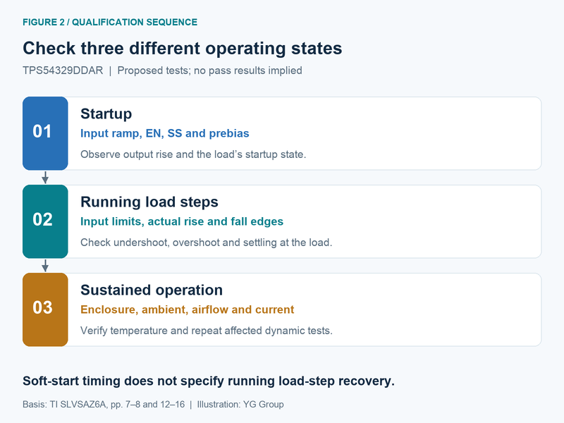
For load-step testing, first verify that the input remains within its intended envelope at the IC. A dip in the upstream source can appear as an output-transient problem. Monitor the input and output together when the behavior is unclear, using appropriate probing for each node. That lets you distinguish a converter/filter issue from a source or interconnect limitation.
Table 4. Conditions that make load-step results comparable
| Test detail | Record explicitly | Common interpretation error |
|---|---|---|
| Load endpoints | Initial and final current at the board | Comparing a small step with a larger one as if they were equal. |
| Edge rate | Measured rising and falling slew rates | Assuming the load setting reaches the PCB unchanged. |
| Pulse duration | Time at each level and repetition rate | Missing sustained heating or slow recovery. |
| Voltage location | Output capacitor and actual load point | Approving a rail from the easier measurement location. |
| Instrument setup | Probe, ground connection, bandwidth and coupling | Treating pickup or filtering as converter behavior. |
| Board condition | Input, temperature, actual LC values and assembly | Comparing unmatched operating points or different effective capacitance. |
Source: editorial test method derived from the TI typical-characteristics conditions and application guidance. The table specifies evidence to collect and does not imply that these tests have been run.
Test both a transition from a light load and one between two higher-current states when both occur in the product. Repeat at relevant input limits and thermal conditions. Keep a consistent definition of settling: for example, return to the load's allowed voltage band without a later excursion. The exact band comes from the load requirement, not from the appearance of the scope trace.
If the result fails, change one plausible cause at a time. A probe correction, a feedback-route repair, and a capacitor substitution answer different questions. Repeating an identical full test matrix after every cosmetic edit wastes time; skipping the affected tests after a functional change loses the evidence needed to approve it. Tie the retest to the mechanism you changed.
There are useful alternatives in the same broad converter class, but the model number alone does not show whether an existing circuit can accept one. A change in switching behavior or current capability can alter the filter, thermal result, and load-transient response even when the package name looks familiar.
Table 5. Four related converters for a focused selection comparison
| Exact related model | Published comparison point | When it deserves attention | What still needs qualification |
|---|---|---|---|
| TPS54329EDDAR | 3 A, 4.5–18 V; 650 kHz family with Auto-Skip Eco-mode | Light-load efficiency changes the system priority | Light-load waveforms, transitions, exact pinout and filter suitability. |
| TPS54328DDAR | 3 A, 4.5–18 V; nominal 700 kHz with Eco-mode | Compare a different switching and light-load arrangement | Frequency-dependent ripple, mode transitions and LC selection. |
| TPS54327DDAR | 3 A, 4.5–18 V; nominal 700 kHz D-CAP2 | Compare a nearby current class with different switching frequency | Electrical limits, pin functions, filter and thermal behavior. |
| TPS54229DDAR | 2 A, 4.5–18 V; nominal 650 kHz D-CAP2 | The verified load requirement is lower | Current peaks, inductor choice, thermal margin and full circuit compatibility. |
Sources: TI exact-part pages for TPS54329EDDAR, TPS54328DDAR, TPS54327DDAR, and TPS54229DDAR. This is a selection comparison, not a completed replacement qualification.
The E in TPS54329E is meaningful here; it identifies a different device with an Eco-mode feature, not merely a packaging choice for TPS54329. A design that prioritizes light-load efficiency may find that useful. A design sensitive to changes in switching behavior must evaluate the corresponding waveforms instead of assuming a one-way improvement.
The TPS54229 option makes a different tradeoff. Its lower current capability may be appropriate if the load envelope supports it, but a comfortable average current is insufficient evidence. Include the largest operating and startup demands, then assess the associated filter and temperature. Reducing current capability should be a deliberate design decision rather than a response to whichever part is easiest to order.
For TPS54329DDAR, the strongest case is a rail whose input and current envelope fits the device, whose LC network follows a defensible design, and whose prototype passes the actual load transitions. D-CAP2 and integrated MOSFETs simplify the circuit. The selection becomes convincing when the voltage budget, effective capacitance, current waveform, layout, and thermal evidence agree.