
Susanna Feng




STM32H743ZGT6 has 1 MB of internal user Flash, organized as two 512 KB banks. The G density code identifies 1 MB; I identifies 2 MB. A family description saying “up to 2 MB” covers multiple devices and does not change the G part's capacity. ST's DS12110 Table 2, ordering information, and exact product entry agree on this distinction.
No. Check the bytes and regions actually programmed into Flash using the release build and final programming artifacts. Include code, constants, initialized-data storage, assets, custom loader, image metadata, and persistent-data reservations as applicable. File-format overhead or debug information can make a workstation file's size misleading. Also budget planned growth and any second retained firmware image before declaring the 1 MB allocation sufficient.
No. The two banks together provide the specified 1 MB; they do not add capacity beyond it. Two complete firmware copies, their metadata, any custom loader, and persistent data must all fit the validated layout. A positive total-space calculation is only an initial screen: bank placement, erase boundaries, boot behavior, rollback, and interrupted-update recovery still need implementation and testing.
The STM32H743ZIT6 comparison increases Flash from 1 MB to 2 MB. DS12110 lists the same H743 RAM-region allocation for the G and I densities. It therefore does not solve a shortage of runtime buffers by itself. Review the required RAM region, DMA access, cache behavior, and any external-memory plan separately from the nonvolatile-storage budget.
It can, when the architecture gives it a defined role such as storing assets or staging an update. The H743 includes a Quad-SPI interface with memory-mapped operation. External memory still requires appropriate pins, routing, initialization, programming, and a recovery strategy; it is not automatically interchangeable with internal Flash. Measure the intended access behavior if runtime code or data depends on it.
Compare the complete release budget and update requirements first. For STM32H743ZIT6, verify the exact package and pin configuration, firmware memory definitions, bootloader assumptions, persistent-data placement, silicon revision, and applicable operating limits and errata. The shared LQFP144 format makes it a relevant comparison, but it does not constitute a validated substitution for a specific board. Record the evidence that justifies the change.
Author: Susanna Feng
Category: 芯片选型与替代 / MCU与MPU选型
STM32H743ZGT6 has 1 MB of internal Flash, arranged as two 512 KB banks. It can suit a Cortex-M7 controller whose complete firmware, persistent data, and update strategy fit that capacity with room for planned changes. The decision turns on what must remain stored at the same time. A single application can fit comfortably while two copies of that application cannot. Start with the release memory budget, then compare the 2 MB STM32H743ZIT6 if the budget demands it.
A development board running a convincing demonstration answers a useful question: the software concept works. It does not settle the memory size for the production controller. The demonstration might omit the recovery loader, language files, diagnostic interface, or second firmware image that the shipped product eventually needs. It might also use a different Flash-density variant.
At the selection review, I would ask for the complete release budget before approving the G-density part. A 1 MB device can be a sensible match for a bounded control application. A product expected to accumulate networking features, display assets, and remote recovery requirements needs a different conversation. The relevant distinction is the software that must coexist, not whether the processor belongs to a high-performance family.
Consider an industrial controller that acquires measurements, runs a control algorithm, and reports status over a network. Its arithmetic can justify a Cortex-M7 even when the firmware is relatively compact. Now add a local graphical interface and an update requirement that preserves the previous release until the new one proves healthy. Neither change necessarily demands a faster core, but both can change the nonvolatile-memory budget substantially.
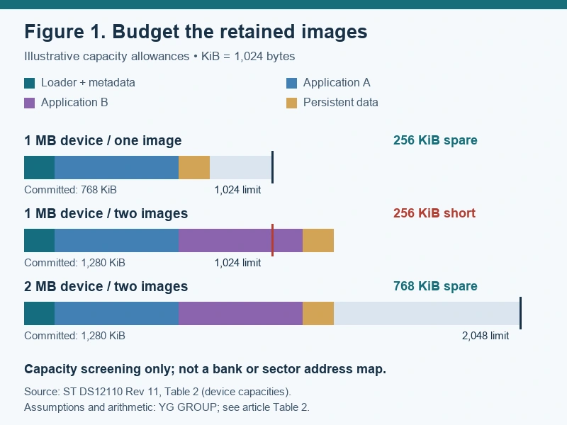
*Figure 1. The second image changes the density decision. Original YG GROUP capacity calculation from Table 2; physical capacities from [ST DS12110](https://www.st.com/resource/en/datasheet/stm32h743zi.pdf). Values are hypothetical allocations, not measured firmware sizes or a bank-address map.* *Figure 2. Three memory questions to settle independently. Original YG GROUP conceptual workflow based on [ST DS12110, Table 2 and sections 3.3, 3.6, 3.14 and 3.15](https://www.st.com/resource/en/datasheet/stm32h743zi.pdf). This is a design-review aid, not a validated software architecture.*Select the Flash density around the maintenance strategy as well as the initial application. Removing the recovery path to make a prototype fit changes the product's service behavior. That can be a valid engineering tradeoff, but it should be an explicit product decision, with the software and service teams agreeing on what happens after an interrupted update.
The examples below are capacity exercises for that discussion. They are not measured firmware sizes, validated linker scripts, or instructions for allocating physical Flash addresses.
ST's DS12110 covers several STM32H742 and STM32H743 variants. Its family headline advertises up to 2 MB of Flash. The ordering information resolves the individual part: G identifies 1 MB, while I identifies 2 MB. For this model, Z specifies 144 pins and T specifies the LQFP package. The suffix 6 identifies the −40°C to +85°C temperature option in the ordering diagram. ST DS12110, Table 2 and ordering information.
The exact STM32H743ZGT6 entry in ST's store independently identifies the 1 MB part and its LQFP144 package. That exact-code entry is more useful for checking an order line than a distributor description copied from a family overview. The family maximum remains useful context, but it cannot enlarge the memory specified for G.
Table 1. Identity details that change the selection decision. Source: ST DS12110 Rev 11, pp. 19–22, 210, 324–325 and 346; compiled by YG GROUP.
| Item | STM32H743ZGT6 fact | Practical consequence |
|---|---|---|
| User Flash | 1 MB total; two 512 KB banks | Budget every simultaneously retained image against 1 MB |
| Processor | Arm Cortex-M7 with single- and double-precision FPU | Compute requirements and storage requirements are separate decisions |
| Package | LQFP144; 20 × 20 mm body, 0.5 mm lead pitch | Body size is not the complete PCB footprint or courtyard |
| GPIO count | 114 in the Z package | Family claims of up to 168 I/Os do not apply to this package |
| Temperature option | Suffix 6: −40°C to +85°C ambient ordering range | Junction temperature still requires a thermal check |
| Highest CPU frequency | Up to 480 MHz on revision V under the specified operating conditions | Do not apply the headline to every silicon revision or thermal condition |
The G-to-I change is a memory-density distinction. It does not describe the silicon revision, and it does not by itself establish the operating clock. DS12110 separates revision Y and revision V electrical characteristics. Table 2 notes that the 480 MHz maximum applies to revision V; the revision V operating table ties that mode to VOS0, the LDO supply configuration, and a maximum junction temperature of 105°C.
For a Flash-capacity decision, this means a larger density is not a substitute for checking the supplied silicon and the board's operating conditions. It also means a part should not be rejected as too small simply because its 1 MB density looks modest beside its processing capability. A computationally demanding algorithm may have a compact executable. A modest user interface can consume substantial storage through fonts and images.
Keep those distinctions visible on the bill of materials. If the schematic uses a short family label but purchasing and firmware use complete codes, the density can get lost between teams. The release record should state the full part number, the approved memory layout, and the image variant that belongs on it.
Use the executable and map report produced by the intended release configuration. A file's size on a workstation is not automatically the number of bytes that the programmer writes into user Flash. Debug information, address gaps, checksums, and container headers can make different file formats report different sizes. Conversely, initialized data used in RAM can require an initial copy stored in nonvolatile memory.
For each programmed region, identify what it contains and which build artifact supplies those bytes. Count executable code, constants, startup data, application assets, and any other programmed payload. Identify separately the space reserved for a custom bootloader and persistent settings. If a signing or packaging step adds information that is stored on the device, include that final representation rather than only the unsigned application build.
Do this with the features intended for shipment enabled. A networking demonstration without the production security configuration is not the same budget as the eventual release. A display demo with one language does not establish the storage needs of a multilingual product. These are examples of changes to measure, not claims that any particular software library has a predictable footprint.
A reserve is more credible when it names what might use it. Planned diagnostics, an additional protocol, and another set of display assets are different growth items. Some can be estimated from trial builds; others need a conservative allocation until implementation exists. The reserve should be revisited when those features move from estimates into the actual image.
For the capacity calculations in this article, 1 KiB means 1,024 bytes. The device's 1 MB Flash density is represented as 1,024 KiB, and the 2 MB comparison as 2,048 KiB. The rounded allocations in Table 2 are deliberately simple. They demonstrate how an update requirement changes the result while holding the application size constant.
Table 2. Illustrative internal-Flash budgets, in KiB. Source: YG GROUP arithmetic using the 1 MB and 2 MB capacities in ST DS12110, Table 2. These are aggregate capacity allowances, not physical bank or sector layouts.
| Capacity allowance | 1 MB, one image | 1 MB, two images | 2 MB, two images |
|---|---|---|---|
| Custom loader and recovery metadata | 128 | 128 | 128 |
| Application A, including its assets and image metadata | 512 | 512 | 512 |
| Application B, including its assets and image metadata | 0 | 512 | 512 |
| Persistent-data allowance | 128 | 128 | 128 |
| Total committed capacity | 768 | 1,280 | 1,280 |
| Device capacity | 1,024 | 1,024 | 2,048 |
| Arithmetic margin or shortfall | 256 spare | 256 short | 768 spare |
The single-image example leaves 256 KiB on the 1 MB device. Adding a second 512 KiB image changes that to a 256 KiB shortfall, without adding one feature to the application. The 2 MB part passes this aggregate capacity exercise, but a positive total margin still does not prove that the chosen loader, bank arrangement, and data placement will work.
Free space also has a location, and that location can change what you can do with it. A design can have enough total unused capacity yet lack the contiguous or independently erasable region required by its updater. The next engineering step is to turn the budget into an exact layout using the reference manual, linker configuration, and bootloader implementation. Keep the arithmetic screen and the implementation review distinct.
ST describes two independent Flash banks in the G-density device, each with 512 KB of user Flash. Their combined capacity is the specified 1 MB. A second bank can be useful to the update architecture, but it is not an additional 1 MB waiting outside the advertised capacity. ST DS12110, p. 19 and section 3.3.1.
Before reserving an A/B arrangement, write down what each copy must contain. Does each application slot carry its own vector table, integrity information, assets, and version metadata? Does a shared data structure remain readable after rollback? Where does the loader remember that a new image has been accepted? These questions determine stored bytes and state transitions, so they belong in the capacity review.
Two banks are a hardware organization; a recoverable update is a complete software behavior. A product can need recovery without keeping two complete application copies internally. It can also retain two copies and still recover badly if the selection metadata or persistent-data migration is unreliable. Capacity enables options; it does not validate them.
A service-port update may be acceptable for equipment maintained by trained staff. A remotely installed controller may require an older working image to remain available until a new one has completed a health check. Another design may stage a candidate image in external memory and copy it internally through a protected recovery path. Each approach moves the storage and validation work to a different place.
Table 3 compares these architectures as engineering choices. It does not claim that ST provides a finished implementation for any of them, and it does not prescribe boot-option settings. The correct choice depends on the permitted downtime, physical access, power-interruption behavior, and product support model.
Table 3. Update choices and their memory consequences. Source: YG GROUP engineering analysis based on the internal Flash, boot, and external-memory capabilities described in ST DS12110, sections 3.3, 3.4, 3.14 and 3.15.
| Update approach | Capacity implication | Recovery question to resolve |
|---|---|---|
| One internal application, service-assisted recovery | No second full internal application allocation | Can the required service interface remain usable after interruption? |
| Two internal application copies | Reserve both complete images plus loader and persistent state | Can the loader select, validate, confirm, and roll back reliably? |
| Candidate image staged externally | Saves internal staging space but requires external storage and handling | Can recovery proceed if copying stops midway? |
| External assets with internal application | Reduces internal asset storage, not automatically application-code storage | Are asset versions consistent with the selected firmware? |
| Feature reduction to retain 1 MB | Frees capacity only after an actual rebuilt image demonstrates it | Is the reduced function acceptable throughout the product's service life? |
Test interruptions at the state changes that matter: receiving a candidate, erasing a target region, writing the image, changing selection metadata, and accepting the new release. That test plan produces more useful evidence than repeatedly updating a powered board under ideal conditions. It also reveals whether the reserved metadata area is sufficient for the intended recovery mechanism.
Keep security and recovery claims separate. An integrity check can detect accidental corruption, while authenticating an update requires a defined trust mechanism. Neither a dual-bank description nor spare Flash establishes that mechanism. Budget the implementation the product actually uses, then review its security behavior separately from the capacity calculation.
Calibration values and configuration records may occupy little logical data, but their storage design can consume a meaningful Flash allocation. A recoverable record scheme may keep older copies, version identifiers, and spare erase space. The budget should reflect those physical reservations, not just the few bytes in the active configuration structure.
Write frequency also matters. DS12110 gives a minimum Flash endurance of 10 kcycles for the stated suffix-6 junction-temperature range, guaranteed by characterization. Its retention figures have explicit temperature and cycling conditions: 30 years after 1 kcycle at 85°C ambient, or 20 years after 10 kcycles at 55°C ambient. Those are conditional specifications, not a single universal retention lifetime. ST DS12110, Table 141, p. 237.
The practical conclusion is to distinguish occasionally changed settings from continuous event recording. If a controller produces frequent logs, moving them to a suitable separate storage device can be an architectural choice even when internal Flash has unused bytes. More capacity alone does not establish that the write pattern, erase distribution, or retention requirement is acceptable.
For configuration data, define the expected update frequency and the recovery behavior after loss of power. Decide which information must survive a firmware rollback and how old software handles a newer data format. These details can change the number of records or regions retained, which feeds directly back into the memory budget.
Avoid spending the last available region twice. A planning spreadsheet can easily describe the same free capacity as both future application growth and emergency logging space. Give every allowance a single owner and a stated purpose. Shared capacity can be a deliberate policy, but the conditions for reclaiming it should be written down before production.
The STM32H743 contains several RAM regions, with different connections and roles. DS12110 lists 512 KB of AXI SRAM, D2-domain SRAM blocks of 128 KB, 128 KB and 32 KB, 64 KB in the D3 domain, 64 KB of ITCM, 128 KB of DTCM, and 4 KB of backup SRAM. The H743 G- and I-density columns have the same listed RAM allocation. ST DS12110, Table 2 and section 3.3.2.
Therefore, moving from STM32H743ZGT6 to STM32H743ZIT6 does not by itself add RAM for a frame buffer, network buffers, or a larger algorithm workspace. It adds internal Flash capacity. If the application fails because a working buffer cannot fit in its required RAM region, the proposed Flash upgrade addresses the wrong constraint.
A graphical application illustrates the difference. Compressed artwork stored in Flash is not the same allocation as the pixels needed for a live frame buffer. As a simple uncompressed example, a 480 × 272 image at 16 bits per pixel requires 261,120 bytes, or 255 KiB. Two such buffers require 510 KiB before other working data. That is arithmetic for an assumed format, not a claim that any particular display configuration is validated on this board.
The H743's LCD-TFT controller, JPEG codec, and graphics-related hardware can support useful design options, but the buffers still need an appropriate location and access path. A peripheral's presence in the feature list does not make every memory region equally reachable or equally suitable. The manufacturer's bus-matrix diagram is the starting point for that placement review.
For time-critical routines, TCM can be valuable. For DMA transfers and shared peripheral buffers, the access paths, cache policy, and memory attributes need attention. Do not combine all RAM blocks into one fictional contiguous buffer, or assume that a buffer accessible to the CPU is automatically accessible through every DMA controller.
The next measurement depends on which resource is running out. If the release image is too large, compare Flash options. If the working set is too large, revisit RAM placement or external memory. If deadlines are missed, measure the execution and data paths under the intended workload. These problems can coexist, but they need different evidence.
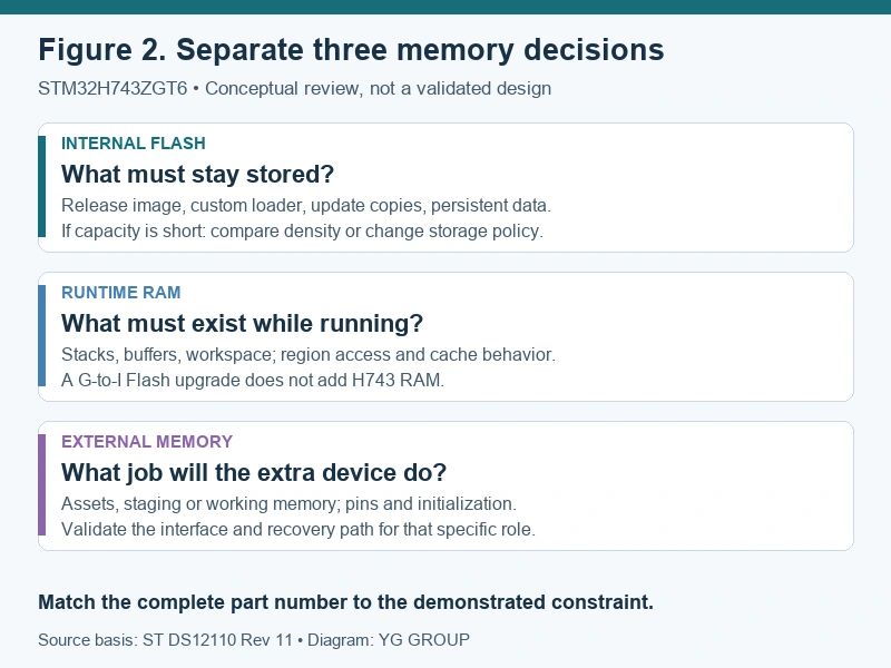
The H743 provides a Quad-SPI interface and a flexible external memory controller. The Quad-SPI description includes memory-mapped operation, and the FMC supports several external memory types. These features give a designer choices for assets, staging storage, or working memory, subject to package pins and the particular interface configuration. ST DS12110, sections 3.14 and 3.15.
Give the external device a named responsibility before adding its capacity to the design budget. Storing a large, mostly static asset set externally is easier to reason about than describing external Flash as an unspecified reserve for whatever later overflows. Likewise, a staging device needs a defined image format and recovery path. Naming its role makes the capacity calculation and the validation work concrete.
External capacity also changes the board. It consumes pins, requires suitable power and signal routing, and introduces a component that must be initialized and programmed. If code or data is fetched through that interface at runtime, access behavior and performance under contention need measurement. Internal and external storage should not be treated as interchangeable merely because software can address both.
The package choice matters here. DS12110 explicitly excludes SDRAM support on the 100-pin packages. A move to a smaller package therefore needs more than a recount of spare GPIOs. It must preserve the specific external-memory function the architecture depends on. Even on a package supporting the interface, multiplexed pins may compete with other required peripherals.
When a design already uses external storage, placing assets or an update candidate there may be worth evaluating. When it does not, compare the total integration effort with the same-package 2 MB MCU option. The useful comparison includes board changes, loader complexity, production programming, and maintenance behavior. A unit-price difference alone cannot answer that engineering question.
STM32H743ZIT6 is the first comparison when the primary issue is internal Flash capacity in the same package format. The other parts below help separate density from package and I/O requirements. They are documented related models, not four approved replacements for an existing board.
Table 4. Four related STM32H743 ordering codes. Source: ST DS12110, Table 2 and ordering information, with exact-code links in each row. GPIO figures are package counts, not an assurance that every desired peripheral can be used simultaneously.
| Related model | Internal Flash | Package and GPIOs | Comparison value and boundary |
|---|---|---|---|
| STM32H743ZIT6 | 2 MB | LQFP144; 114 GPIOs | Same package format and more Flash; verify layout, firmware, revision, and qualification before substitution |
| STM32H743VGT6 | 1 MB | LQFP100; 82 GPIOs | Smaller package comparison; new board mapping, fewer exposed signals, and no SDRAM support on this package |
| STM32H743IGT6 | 1 MB | LQFP176; 140 GPIOs | More exposed I/O without increasing Flash; useful when interfaces, rather than code size, drive selection |
| STM32H743BIT6 | 2 MB | LQFP208; 168 GPIOs | Larger-package historical comparison; ST lists this exact code as NRND, so it is not a fresh-design recommendation |
The NRND status in the last row was checked on ST's product page on September 23, 2026. It should be rechecked for any sourcing decision. That row is useful precisely because an attractive resource count can coexist with a lifecycle reason to avoid starting a new design around it. It is not presented as evidence that the part is unavailable or discontinued.
For the same-package ZIT6 comparison, resist calling the change automatic. Review the memory definition used by the build, programming range, bootloader assumptions, persistent-data placement, silicon revision, and applicable errata. A design that only uses the lower-density allocation may have a different migration task from one that immediately expands into additional space. Neither case is established by a matching package name alone.
The IGT6 example makes the opposite point: a larger package does not solve an oversized firmware image when the Flash-density code remains G. It can make more signals available, yet retain the same 1 MB capacity. Keeping the two axes separate prevents an expensive board change from being justified by a storage problem it does not fix.
A useful capacity review ends with artifacts that another engineer can inspect. Keep the exact build configuration, programmed-image description, memory map, and update-layout definition together. When the next release grows, the team should be able to identify which category changed instead of reconstructing the original assumptions from a spreadsheet total.
Table 5. Evidence that turns a density choice into a release decision. Source: YG GROUP editorial verification method, derived from the memory, package, and operating boundaries in ST DS12110.
| Evidence | What it should show | Decision it supports |
|---|---|---|
| Complete BOM code and silicon record | Approved density, package, temperature option, and relevant revision | Firmware is being qualified for the device actually purchased |
| Release build and map report | Programmed regions, included features, initialized data and assets | The application budget uses the shipping configuration |
| Final image format and layout | Loader, image metadata, data reservations, bank and erase boundaries | Positive aggregate margin can be implemented as a valid layout |
| Update and recovery results | Behavior at interrupted erase, write, selection and confirmation stages | The claimed maintenance path works under the tested conditions |
| Growth and data-workload review | Named future allocations, setting-write frequency, log placement | Remaining capacity has a defined purpose and is not counted twice |
There is no universal utilization percentage that makes every 1 MB project safe. A stable, narrowly scoped controller and a feature-expanding connected product have different growth expectations. What matters is whether the remaining allocation is sufficient for the changes the team intends to support and whether those changes have been estimated in a credible way.
A practical sign-off can be brief: the current release occupies these regions; this update strategy retains these copies; persistent data uses this reservation; planned additions have this allowance. If one of those statements is missing, “the binary fits” leaves the important question unanswered. If all are backed by the build and tests, retaining the 1 MB device can be a deliberate, defensible decision.
STM32H743ZGT6 is worth considering when the complete 1 MB budget works for the control application and its service life. Its Cortex-M7 processing capability does not require a large firmware image, and the G-density choice can fit a focused design. The justification should be a measured release image and an implementable memory layout.
When a second retained image, expanding assets, or planned features consume the available margin, compare STM32H743ZIT6 early. When the problem is working RAM or exposed signals, pursue that constraint directly. The strongest reason to choose 1 MB is that the intended product fits it, including how that product will be updated and maintained.