
Georgia Huang



3 views

| Picture | Part Number | Manufacturer | Stock | Action |
|---|---|---|---|---|
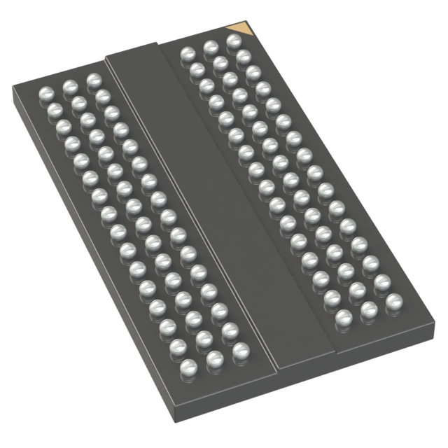 | MT41K64M16TW-107:J | Micron | 9,250 | |
 | MT41K64M16TW-107:J TR | Micron | 2,950 |
No. It is a 1Gb device organized as 64M × 16, equivalent to 128 MiB. A board can combine multiple devices, so total system capacity must be calculated from the actual population and organization.
Micron's speed-bin table permits lower-speed operating points, including CL6/CWL5 at a 2.5 ns clock period. Use the documented combination, recalculate the remaining timing requirements, and follow the required initialization or frequency-change procedure. Slower operation is not permission to use reserved settings.
No. Approval also depends on the ball map, voltage conditions, timing combinations, controller support, initialization, thermal behavior, and board validation. Matching a few catalog fields is the beginning of the comparison.
MT41J64M16JT-15E:G is a Micron 1Gb DDR3 SDRAM organized as 64M × 16, with a 96-ball JT package and a DDR3-1333 speed grade. Selecting it requires matching the controller's memory geometry, supply, clock period, and legal timing settings. The -15E rating supports a 1.5 ns clock period with CL9; it does not approve every controller configuration or establish replacement compatibility. Micron datasheet, pp. 1–2 and 72
A parts list may describe this device simply as “1Gb DDR3, 667 MHz.” That description leaves several decisions unresolved. Is the board configured for the correct number of rows and banks? Does its firmware express a timing field in clocks, nanoseconds, or an encoded value? Will the controller maintain the required refresh rate at the highest package temperature?
For a maintenance purchase or a revised bill of materials, the useful output is a documented memory configuration tied to the complete ordering code. Start with the physical device, then work through the timing and qualification evidence.
The Micron ordering information separates organization, package, speed, temperature option, and die revision. The final :G identifies the device revision; it is separate from the revision letter of the datasheet. The absence of an IT temperature suffix corresponds to the commercial option. An AIT or AAT automotive document must not be used to assign an automotive temperature range to this commercial ordering code. Micron's archived FBGA decoder also lists the complete MT41J64M16JT-15E:G identifier.
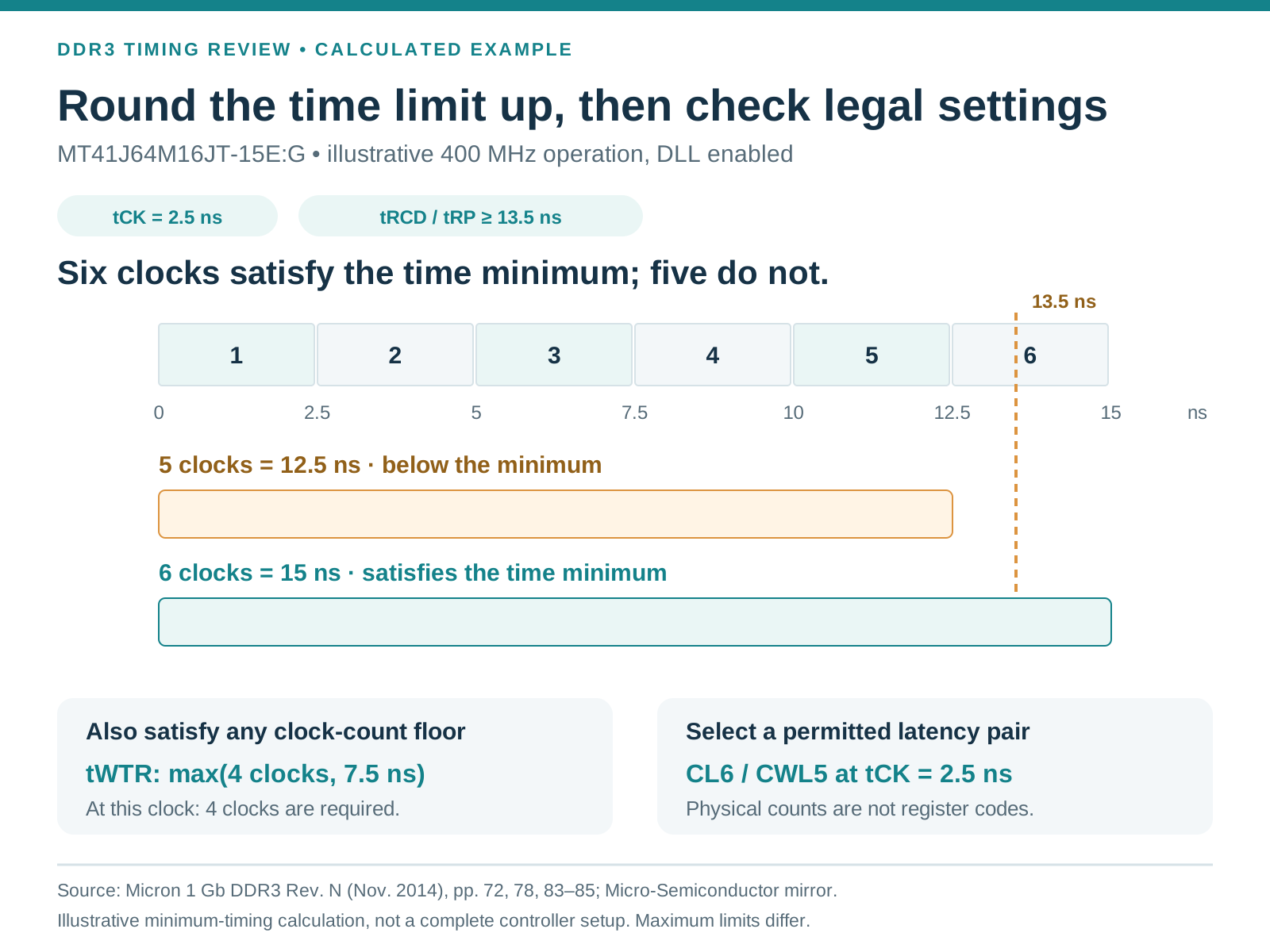
**Figure 1. Round the time limit up, then check legal settings.** Illustrative MT41J64M16JT-15E:G timing check at 400 MHz, tCK = 2.5 ns, with the DLL enabled. A 13.5 ns minimum requires six clocks; tWTR also has a four-clock floor, and CL6/CWL5 is a separately permitted latency pair. These are physical timing requirements, not a complete register image. Maximum intervals need different rounding treatment. Sources: [supporting source 1](https://www.micro-semiconductor.com/datasheet/10-MT41J64M16JT-15E-AIT-G.pdf). **Figure 2. Change frequency only in a permitted state.** Conceptual eligibility review for a frequency change after MT41J64M16JT-15E:G initialization. Use self-refresh or the specified precharge power-down conditions and follow the applicable sequence, exit and DLL requirements. The diagram supplies no register programming recipe or timing sequence. DLL-disabled operation has separate restrictions and is not covered by the normal-mode timing guarantee. Sources: [supporting source 1](https://www.micro-semiconductor.com/datasheet/10-MT41J64M16JT-15E-AIT-G.pdf).| Selection item | MT41J64M16JT-15E:G baseline | Practical check |
|---|---|---|
| Organization | 64M × 16; eight banks | Confirm the controller's width and address mapping |
| Density | 1Gb, equivalent to 128 MiB of storage | Do not enter 1GB as the capacity of one device |
| Address geometry | 8K rows, 1K columns, eight banks; 2KB page | Match the controller's row, column, and bank configuration |
| Package | JT: 96-ball FBGA, nominal 8 × 14 mm | Compare the ball map, footprint, assembly drawing, and height allowance |
| Supply | VDD and VDDQ: 1.425–1.575 V, nominal 1.5 V | Check both rails and their required tracking |
| Temperature | Commercial case-temperature range, 0–95°C, with extra refresh requirements above 85°C | Use package temperature and the correct refresh policy |
These values come from Micron's organization table, package drawing, electrical conditions, and temperature guidance. The capacity conversion is arithmetic: 64 × 2²⁰ locations × 16 bits ÷ 8 = 128 × 2²⁰ bytes. The datasheet also requires VDDQ ≤ VDD and equal rail levels for valid AC timing parameters. Micron datasheet, pp. 2, 17, 24, 28 and 44
For purchasing, preserve the punctuation and full suffix in the approved BOM and supplier documentation. A short package marking is a separate identifier: Micron notes that its FBGA marking differs from the full part number and provides a decoder. Package resemblance alone does not identify the speed or revision. Micron ordering information, p. 2
DDR transfers data on both edges of the data strobe. At the -15E grade's minimum average clock period of 1.5 ns, the clock frequency is approximately 666.7 MHz and the data rate is approximately 1,333 million transfers per second per data pin. Thus, a catalog's rounded “667 MHz” and the designation DDR3-1333 can describe the same speed grade; they are different quantities.
The calculation is:
Micron's Table 51 lists -15E as 9-9-9: CL9, tRCD of 13.5 ns minimum, and tRP of 13.5 ns minimum at this operating point. The neighboring -15 speed grade is 10-10-10, with 15 ns values. Keeping the E in the order code therefore matters even though both grades appear under DDR3-1333. Micron datasheet, pp. 12 and 72
CL is the interval between an internal READ command and the first output data. It is not the complete processor-to-memory access latency. With additive latency enabled, the command-to-data read latency is RL = AL + CL. Opening a row, changing rows, bus turnaround, refresh, and the controller's own scheduling can add other delays. A “13.5 ns memory” description cannot predict an application's access time. Micron datasheet, pp. 137, 140–142 and 154–157
For minimum timing limits specified in nanoseconds, Micron directs the designer to divide by the actual average clock period and round a noninteger result upward. Where a parameter also has a minimum number of clocks, satisfy both limits. Maximum intervals require the opposite rounding direction: rounding them upward could exceed the permitted time. Micron timing notes, pp. 83–85
Consider an illustrative configuration using this part at 400 MHz, equivalent to 800 MT/s, with the DLL enabled and an average clock period of 2.5 ns. This is a timing calculation, not a validated controller setup:
| Item | Calculation or allowed setting | What it establishes |
|---|---|---|
| tRCD, using the -15E 13.5 ns limit | Ceiling of 13.5 ÷ 2.5 = 6 clocks | Six clocks provide 15 ns |
| tRP, using the same 13.5 ns limit | Ceiling of 13.5 ÷ 2.5 = 6 clocks | Five clocks would provide only 12.5 ns |
| tWTR | Greater of 4 clocks or 7.5 ns | Four clocks remain necessary although 7.5 ns equals three clocks |
| CL and CWL | CL6 and CWL5 are allowed at tCK = 2.5 ns | The legal pair must be selected from the speed-bin table |
The limits and permitted pair are specified in Table 51 and Table 55. This example deliberately uses one conservative set of time limits; it is not a complete controller register image. Micron datasheet, pp. 72, 78 and 83–84
The register check is essential. A controller cannot choose an arbitrary CL merely because CL multiplied by tCK exceeds a time minimum. Micron couples each permitted CL/CWL pair to an allowed clock-period range and marks other combinations reserved. At the 1.5 ns operating point, CL9 pairs with CWL7. At 2.5 ns, CL6 pairs with CWL5. Copying CL9/CWL7 into the slower configuration would ignore that table.
Also confirm how the particular controller encodes each field. A calculated six-clock requirement is a physical timing requirement, not necessarily the value “6” to write into a register. The controller's own programming documentation must resolve its units, offsets, and supported values.
CL, tRCD, and tRP describe only part of the command schedule. The -15E table also specifies tRAS, the minimum active-row time, and tRC, the same-bank row-cycle interval. Activation of different banks is constrained by tRRD and the four-activate window, tFAW. Micron lists different tRRD/tFAW conditions for x16 devices with a 2KB page and for x4/x8 devices with a 1KB page. A configuration copied from a same-density x8 memory can therefore be wrong for this x16 device. Micron datasheet, pp. 72, 78 and 154–155
The firmware review should account for the complete command path: write recovery, read-to-precharge, read/write turnaround, mode-register update delays, and refresh recovery. For this 1Gb density, Table 55 gives a minimum tRFC of 110 ns. That interval is distinct from the periodic refresh interval, tREFI; confusing the two fields would change the controller's behavior substantially. Micron datasheet, pp. 78–81
Temperature belongs in this same review. The normal external refresh period is 64 ms, corresponding to approximately 7.8 µs between refreshes on average. Above 85°C case temperature, and within the device's supported range, the refresh period is reduced to 32 ms, approximately 3.9 µs on average. Self refresh requires the appropriate SRT or ASR setting for the extended range; both must not be enabled simultaneously. A successful room-temperature boot does not establish correct high-temperature retention behavior. Micron datasheet, pp. 79, 118, 143 and 179
Timing values become useful only after the memory has been initialized correctly. Micron's power-up sequence includes controlled supplies and RESET#, a CKE delay, programming MR2, MR3, MR1 and MR0, DLL reset, and ZQ calibration. Normal operation waits for both DLL locking and the initial calibration requirements. This is more than selecting a frequency and issuing the first read. Micron initialization sequence, pp. 131–132
If the operating clock changes after initialization, use the permitted sequence. Micron allows frequency changes in self refresh or under the specified precharge power-down conditions; changing the clock freely during normal accesses is not permitted. DLL-disabled operation also has separate restrictions and is not covered by the normal-mode timing guarantee. Micron datasheet, pp. 120–125 and 138–139
The board review should connect these firmware decisions to physical evidence. Confirm the two byte lanes of the x16 device, their DQS connections, reference supplies, termination strategy, and ZQ resistor. The datasheet specifies a 240 Ω ±1% external ZQ reference resistor for calibrated output-driver and termination impedance. Write leveling, when required by the topology and controller, aligns the strobe with the clock at the DRAM; it does not remove the need to check routing and signal margins. Micron datasheet, pp. 17, 20–21, 126–130 and 153
For qualification, record the tested board revision, controller configuration, voltage and temperature conditions, training results, sustained read/write testing, and relevant reset or low-power transitions. These are proposed acceptance checks, not test results for a YG Group sample or an existing customer board.

Micron's Lattice partnership page identifies MT41K64M16TW-107:J as a 1Gb, 64M × 16 DDR3L SDRAM used on the Certus-NX evaluation platform. The matching density and bus width make it a relevant comparison candidate. Qualification on that named platform does not validate its use in a different board designed for MT41J64M16JT-15E:G. Micron's Lattice platform information
The DDR3L designation does not answer the replacement question. Obtain the candidate's applicable electrical specification, package drawing, speed-bin table, temperature conditions, and revision information. Compare its supported supply modes with the board's actual rails, and confirm that the controller can program a legal configuration. Any differences in package, assembly process, training, or power behavior belong in the change-control record before approval.
For a purchase of the original part, request the complete ordering code, lot and date-code information, traceability documentation, packaging condition, and any applicable manufacturer notices. Make availability and lifecycle decisions from current, order-specific evidence rather than the age or continued online presence of a datasheet.
For MT41J64M16JT-15E:G, the decisive selection document is the configuration record: exact part identity, correctly expressed timing limits, supported CL/CWL settings, temperature-aware refresh, and qualification evidence for the actual board. Keep that record with the approved BOM so the next purchase or revision can be reviewed against the same requirements.
Author: Georgia Huang