
Beebee Chiang



| Picture | Part Number | Manufacturer | Stock | Action |
|---|---|---|---|---|
 | LAN8720A-CP-TR | Microchip | 7,230 | |
 | DP83825IRMQRG4 | Texas Instruments | 8,350 | |
| DP83825IRMQR | Texas Instruments | 8,010 | |
 | DP83826IRHBR | Texas Instruments | 4,920 | |
 | DP83848IVVX/NOPB | Texas Instruments | 7,860 | |
 | DP83822IRHBR | Texas Instruments | 2,400 |
Not by itself. LAN8720A-CP-TR is a physical-layer transceiver that expects a compatible Ethernet MAC with RMII. It is not a stand-alone Ethernet controller with a host SPI interface. Check the exact MCU's MAC capability, package pin availability, clock input and software support before selecting this PHY. The external connector and magnetics do not provide the missing MAC function.
No. Microchip's ordering system identifies CP as extended commercial operation from 0°C to +85°C. The industrial variant includes the i designation and has a different lower temperature limit. TR denotes tape-and-reel packaging, not a temperature upgrade. The standard CP order uses the 24-pin QFN package. For a product that must operate below 0°C ambient, revisit the exact ordering code instead of relying on the LAN8720A family name.
Not through the shared nINT/REFCLKO pin. In REF_CLK Out mode, the PHY generates a 50 MHz reference from a supported 25 MHz source, and nINT is unavailable. The MCU must accept that reference, and its timing must be checked against the PHY's output-clock-mode requirements. In REF_CLK In mode, an external 50 MHz source clocks both devices and pin 14 can provide the interrupt output.
Article: W38-29
By: Beebee Chiang
Manufacturer: Microchip Technology
LAN8720A-CP-TR is a compact 10/100 Ethernet physical-layer transceiver for a microcontroller that already has an Ethernet MAC and a compatible RMII interface. Its small package and internal core regulator can simplify an Ethernet board, but they do not remove the clock, reset and firmware decisions that make the connection work. An MCU with spare GPIO, SPI or I²C alone is not enough.
The most consequential choice often happens before the first packet: will an external 50 MHz source clock both devices, or will the PHY generate the MCU's reference clock from a 25 MHz source? On this part, the second option uses the pin that otherwise provides the interrupt output. Microchip also requires a MAC-to-PHY timing analysis for that output-clock mode. Microchip DS00002165C, sections 3.7.4 and 5.6.4.
Choose this PHY when the MCU interface, clock arrangement and commercial-temperature suffix fit the product together. Do not decide from “10/100 Ethernet” and package size alone. For a small networked bench instrument or indoor controller, those choices can produce a straightforward design. For a product that needs cold-temperature operation, a dedicated interrupt while using PHY-generated clocking, or a different MAC interface, they can change the shortlist immediately.
The default nINTSEL pull-up selects REF_CLK In, which expects the external 50 MHz reference arrangement. Using the PHY to generate the MAC reference from a 25 MHz crystal requires REF_CLK Out selection with nINTSEL low. Confirm the shared LED/strap circuit and the MCU's clock input before committing the schematic. Merely fitting a 25 MHz crystal does not select the right operating mode or establish device-pair timing compatibility.
The detailed power-pin table in DS00002165C explicitly specifies 1 µF and 470 pF decoupling capacitors in parallel from VDDCR to ground. Use that explicit requirement instead of copying the simplified power drawing literally. The detailed RBIAS description similarly specifies 12.1 kΩ with 1% tolerance. With the internal regulator disabled, an appropriate external core supply and its sequencing are additional requirements; VDDCR is not an optional unused pin.
Link indication does not validate the complete digital or software path. Check the selected RMII clock mode and timing, MCU pin configuration, resolved PHY speed/duplex and matching MAC settings. Then inspect buffers, DMA and the network stack. Reliable MDIO access helps isolate management from packet transfer, while a register snapshot preserves the negotiated state. A 100 Mbps physical link also does not guarantee the application's sustained throughput.
The PHY handles the electrical connection to the cable, including the 10BASE-T or 100BASE-TX line interface. The MAC on the MCU handles the Ethernet frame interface toward the processor. RMII, the Reduced Media Independent Interface, connects those two blocks. The external magnetics and connector complete another part of the link; they do not supply the missing MAC.
This division of work gives a useful first selection test. Check that the chosen MCU package exposes the required RMII signals and that those pins are available in the intended product. A peripheral listed in an MCU family brochure may share pins with a display, memory interface or debug function in the exact package being used. Resolve those conflicts before comparing PHY unit prices or copying an evaluation-board schematic.
The next check is the MCU's reference-clock capability. Does its MAC accept an external 50 MHz RMII clock? Can an appropriate clock be distributed to both devices? Does the intended firmware and board support package assume a different clock source? Those answers explain why a PHY that works on one board may need a different clock arrangement on another board using the same MCU family.
Table 1. First-pass fit for LAN8720A-CP-TR
| Selection question | Verified device boundary | Consequence for the MCU board |
|---|---|---|
| Does the MCU have an Ethernet MAC? | This device is a PHY, not a stand-alone Ethernet controller | A GPIO-only or SPI-only host needs a different architecture |
| Is the MAC interface RMII? | Two-bit RMII transmit and receive data paths | Confirm exact MCU pin availability and peripheral configuration |
| What line speed is needed? | 10BASE-T and 100BASE-TX | A gigabit requirement removes this part from consideration |
| Is the environment suitable? | CP means 0°C to +85°C extended commercial operation | Do not treat this ordering code as the industrial variant |
| Is the board space appropriate? | Standard CP order uses a 24-pin, 4 × 4 mm QFN package | Include the exposed pad, routing and external components in the footprint budget |
| How is management handled? | MDC/MDIO serial management interface | Provide access for identification, configuration and link diagnostics |
Source: Microchip DS00002165C, pages 1, 6–12, 66–70 and 75. Table decisions are engineering implications of those features.
A 100 Mbps negotiated link is not a promise of 100 Mbps application throughput. The processor, memory movement, software stack, packet sizes and application workload all sit outside the PHY's line-rate specification. If the instrument must stream data at a defined sustained rate, plan a system throughput test. Keep that requirement distinct from proving that the PHY establishes a 100BASE-TX connection.
The CP suffix deserves an explicit entry in the bill of materials. The datasheet distinguishes the extended commercial version from LAN8720Ai industrial variants. Tape-and-reel designation TR describes packaging, not a broader operating-temperature rating. For a required ambient temperature below 0°C, this exact CP ordering code is not the qualified choice. Revisit the orderable part and the rest of the board's temperature requirements instead of treating the family name as sufficient evidence. DS00002165C, product identification system, page 75.
LAN8720A has two arrangements that look similar on a block diagram but produce different integration tasks. Both ultimately use a 50 MHz reference for RMII. The distinction is where that reference originates and what happens to pin 14, shared between nINT and REFCLKO.
In REF_CLK In mode, nINTSEL is high, which is also its default pull-up state. A suitable external 50 MHz source drives the PHY's XTAL1/CLKIN input and the MAC's reference-clock input. XTAL2 is unused for this single-ended input arrangement. Pin 14 remains available as nINT, an open-drain interrupt output that needs the appropriate external pull-up.
This is the cleaner starting point when the firmware architecture benefits from a PHY interrupt or the board already has an appropriate clock source. It still requires a distribution and timing review. A common source does not mean the clock reaches both devices at precisely the same instant. Trace delay, buffering, loading and the MCU's timing requirements determine the remaining margin.
Avoid creating two independent nominally 50 MHz sources and assuming that their printed frequency makes them synchronous. The connection requires the timing relationship of the selected RMII architecture. The purpose of the shared reference is to establish that relationship; separate oscillators with similar frequency labels do not establish it.
In REF_CLK Out mode, nINTSEL is low. A 25 MHz crystal, or the supported 25 MHz external clock arrangement, feeds the PHY, which provides a 50 MHz reference to a MAC capable of accepting it. The attractive feature is consolidation of the clock source. The tradeoff is explicit: REFCLKO occupies pin 14, so nINT is unavailable in this mode.
That can be entirely acceptable when firmware polls link status at a suitable interval. It is less attractive when an existing driver expects an interrupt, when link-state response time is tightly constrained, or when the MCU cannot use that external clock arrangement. Include the software behavior in the decision rather than leaving it as a surprise for bring-up.
Microchip states that REF_CLK Out timing is not compliant with the RMII specification and requires a timing analysis of the MAC and LAN8720. This is not a statement that the mode cannot work. It means that selecting it requires checking the actual device pair against its published timing, rather than relying on interface names alone. DS00002165C, pages 28–31.
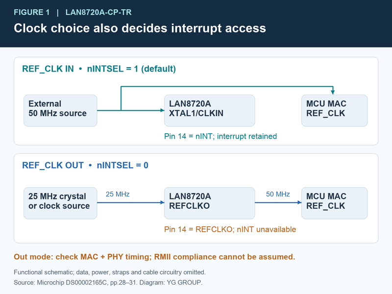
Table 2. Clock mode is a hardware and firmware choice
| Item | REF_CLK In | REF_CLK Out |
|---|---|---|
| nINTSEL state | High; default internal pull-up | Low; deliberately select this mode |
| Source at the PHY | External 50 MHz clock at XTAL1/CLKIN | 25 MHz crystal or supported external 25 MHz clock arrangement |
| MAC reference | Same external 50 MHz source | 50 MHz REFCLKO from the PHY |
| Pin 14 function | nINT interrupt output | REFCLKO; nINT unavailable |
| Main selection benefit | Retains the interrupt and supports shared clocking | Can consolidate the clock-source arrangement |
| Main verification task | Common-reference distribution and both devices' timing | Explicit PHY-output-mode timing analysis plus compatible MCU clock input |
Source: DS00002165C, pages 28–31 and 60–61. These are mode-specific facts; neither column establishes compatibility with an unnamed MCU.
The clock-mode choice changes the relevant timing table. For example, the PHY's receive-data output-valid maximum is 14 ns in REF_CLK In mode and 5 ns in REF_CLK Out mode. The transmit-data setup requirements are 4 ns and 7 ns respectively. These values have different clock references, so the smaller receive-output number is not evidence that one mode is universally faster or easier to route.
Check whether the receiving device sees stable data on both sides of its sampling edge. For traffic from the PHY to the MCU, combine the PHY output timing with the MCU input requirement and the board's relative clock/data delay. For traffic from the MCU to the PHY, start with the MCU output timing and use the PHY's input setup and hold requirements. Treat the two directions separately.
Table 3. Selected RMII timing values at the PHY boundary
| Timing parameter | REF_CLK In mode | REF_CLK Out mode | How to interpret it |
|---|---|---|---|
| Nominal reference period | 20 ns | 20 ns | The reference remains 50 MHz for the RMII interface |
| Receive outputs valid after rising reference edge | 14.0 ns maximum | 5.0 ns maximum | Pair with the MAC input timing and relative clock/data delay |
| Receive output hold from rising reference edge | 3.0 ns minimum | 1.4 ns minimum | Check the MAC hold requirement separately from setup |
| Transmit input setup to rising reference edge | 4.0 ns minimum | 7.0 ns minimum | Data produced by the MCU must meet the selected PHY mode |
| Transmit input hold after rising reference edge | 1.5 ns minimum | 2.0 ns minimum | Include early-arriving data and clock skew in the review |
Source: DS00002165C Tables 5-10 and 5-11, pages 60–61. Timing was designed for a system load of 10–25 pF. This table is not a complete MCU-to-PHY timing budget.
A simple arithmetic example explains why the MCU datasheet is needed. In an assumed same-edge, next-cycle receive analysis for REF_CLK In mode, a 20 ns period minus the PHY's 14 ns maximum output-valid time leaves 6 ns before accounting for MCU setup, clock/data skew and other allowances. That is an illustrative starting expression, not a verified 6 ns board margin. The MCU's actual sampling convention and specifications decide whether that expression applies.
Hold deserves the same attention. Shortening a data trace can help a setup concern while making the earliest data arrival less favorable for hold. A design review should therefore state its clock convention and evaluate both inequalities, not just insist that every connection be “as short as possible.” Good placement simplifies the problem, but it does not replace the timing calculation.
For layout, keep the digital clock path deliberate and avoid routing it through an unnecessarily noisy or circuitous region. Treat the analog cable interface and its magnetics requirements as a separate layout task. A successful timing calculation at the MAC pins does not establish the quality of the Ethernet transmit waveform or the finished product's electromagnetic behavior.
The internal core regulator is a useful integration feature. With the default regulator-enabled selection, it supplies the nominal 1.2 V core through VDDCR. That saves an external core-supply function, but VDDCR still requires its specified decoupling. The pin description calls for 1 µF and 470 pF capacitors in parallel to ground. The exposed VSS pad connects to the ground plane through a via array. DS00002165C, page 11.
The operating-conditions section gives VDDIO as 1.62–3.6 V and the analog supplies VDD1A and VDD2A as 3.0–3.6 V. The I/O supply flexibility is valuable when the MCU interface uses a lower logic voltage. It does not remove the analog supply requirement, permit 5 V digital signals, or allow the MCU to drive an unpowered PHY. Match the rails and startup behavior, not just their nominal voltage labels.
There is a useful document-reading trap here. The simplified power drawing on page 72 marks VDDCR as NC, while the detailed pin table on page 11 explicitly requires decoupling. The pin table also specifies a 12.1 kΩ, 1% RBIAS resistor, whereas the simplified drawing rounds the label to 12 kΩ. Use the explicit VDDCR and RBIAS pin requirements; do not copy the simplified drawing literally. The article's illustrations deliberately avoid reproducing that ambiguous power drawing.
If the internal regulator is disabled through REGOFF, an external core supply is required and its sequencing conditions apply. That choice can make sense in a system with a suitable existing rail, but it adds integration work. Do not disable the regulator because a reference schematic has a pull-up on a shared LED pin unless the resulting power architecture has been checked.
Several pins have two jobs: they set startup configuration during reset and carry another signal afterward. MODE pins select the initial operating mode, PHYAD0 selects the initial address bit, and the LED pins share the regulator and clock selections. Their final logic state depends on the pull network and whatever else is connected to the node.
The default MODE setting advertises the supported 10/100 half/full-duplex capabilities with auto-negotiation. That is a sensible starting point for an ordinary network port. An unintended strap change can produce behavior that looks like a software negotiation problem, so record the intended mode and verify the latched state during bring-up.
Pay particular attention to pull-up domains. Ordinary configuration straps use VDDIO as specified, but the shared LED/nINTSEL and LED/REGOFF arrangements use VDD2A for their high selection. LED polarity and loading therefore belong in the configuration review. A cosmetic LED change can otherwise alter a functional startup decision. DS00002165C, sections 3.7 and 3.8.1, pages 25–32.
Hardware reset and software reset are not interchangeable for every purpose. The strap configuration is established through the hardware startup/reset mechanism, rather than being redefined by an arbitrary software reset. If the wrong hardware selection was latched, first inspect the strap circuit and reset sequence. Repeatedly restarting the driver cannot correct an electrically wrong pull network.
Microchip's power-on timing specifies at least 25 ms from all external supplies reaching 80% to nRST deassertion, at least 100 µs of nRST assertion, and strap setup and hold times of 200 ns and 1 ns around deassertion. The complete power sequencing requirements still apply. These are different constraints, so a single delay inserted at a convenient point in firmware is not automatically equivalent to satisfying them. DS00002165C, pages 58–59.

Make the first software diagnostic a narrow one: can the MCU read sensible PHY identification and configuration registers over MDIO? This separates management access from cable negotiation and application traffic. Use the strap-selected address first. PHYAD0 supplies only the initial low address bit; do not assume the hardware exposes five independent address straps merely because the management protocol has a wider address field.
MDC frequency is another easy place to carry an MCU default into the wrong device. The serial-management timing gives a minimum MDC period of 400 ns, corresponding to a maximum 2.5 MHz. Configure the divider for the actual MCU peripheral clock. A change in system clock can silently change MDC if the divider is left untouched. DS00002165C, Table 5-7, page 57.
After management access works, check the resolved link state and configure the MAC accordingly. A physical link can negotiate successfully while the MCU still uses the wrong speed or duplex setting. The driver needs to carry that result across the PHY/MAC boundary, then establish that packets traverse the intended DMA, buffer and network-stack path.
Some status bits preserve an event until read. The basic status register's link bit is latch-low, so one read can report a previous loss of link rather than the present condition. Follow the register semantics when deciding whether to read again for current status. Conversely, do not scatter unsolicited diagnostic reads of event registers through the code if those reads change what the main driver can observe.
Reserved bits also need their documented treatment. Do not adopt a blanket rule that every reserved field should be written as zero: the special modes register includes a reserved bit specified to be written as one. Use the appropriate masks and required values for the register being changed. That is a small implementation detail with a large debugging benefit because it makes configuration writes reproducible.
A lit link LED is encouraging, but it answers a much smaller question than “does Ethernet work?” It does not establish MCU clock compatibility, correct receive sampling, suitable MAC descriptors, an assigned IP address or a functioning application protocol. Bring the system up in layers so a failure has a short list of plausible causes.
Table 4. Observations that narrow the next investigation
| Observation | Check next | Why this is the useful boundary |
|---|---|---|
| No reliable management response | Power, reset, address, MDC rate, MDIO connections and pull-up | Cable negotiation is not needed to establish basic register access |
| Management works, no cable link | Mode straps, clock source, magnetics, connector and link partner | The host can talk to the PHY, but the physical link still needs investigation |
| Link is up, MAC receives no valid traffic | RMII clock mode and timing, MCU pin selection and MAC configuration | Negotiation alone does not validate the digital data path |
| Traffic fails after speed or duplex changes | Resolved PHY state and matching MAC settings | Both sides of the internal interface must use the same result |
| Works after a reset but not from cold power-up | Supply sequencing, reset timing and strap loading | The initial electrical state differs from an already powered restart |
| Basic packets work, workload misses its target | Buffers, DMA, stack and application processing | PHY line speed is not a system throughput measurement |
Editorial debug sequence based on the device's interface, reset, clock and register functions. It is a diagnostic aid, not a claim that one observation proves one specific fault.
Auto-negotiation should normally be allowed to resolve capabilities at both ends. Forcing a setting on one side while the other side follows a different negotiation path can produce an unexpected duplex result. If a product genuinely needs a forced mode, document the link-partner requirement and test it as a system arrangement. Do not interpret a link LED as confirmation that both ends agree on every operational setting.
Low-power behavior also deserves a workload test. An energy-detect mode can reduce idle consumption, but waking from that mode can lose initial traffic as described in the datasheet. That is different from promising transparent reception of the first application packet or a complete Wake-on-LAN feature. Choose the power mode from the product's acceptable wake behavior, then exercise that behavior with real traffic patterns.
Keep a short startup record for each failing case: supply sequence, reset timing, strap-selected mode, PHY address, register identity, negotiated state and the MCU MAC settings. Compare a cold power-up with a warm restart using the same cable and link partner. Changing several variables at once makes a recovered link difficult to explain and the eventual fix difficult to trust.
A useful release test also changes the order in which the cable and equipment become available. Try power-up with the cable connected, power-up without it, and reconnection after normal operation. These are proposed system tests, not Microchip production tests. They exercise the driver's transitions between no-link and negotiated operation, which a single successful boot does not cover. Preserve the failing sequence if one case behaves differently.
If the clock, package or feature tradeoff does not fit, several different PHYs provide meaningful comparison points. The four devices below come from Texas Instruments and have independently identifiable order codes. They are design candidates for an MCU Ethernet interface, not pin-compatible replacements for the Microchip part.
Table 5. Four related PHY candidates and the requirement each can address
| Comparison candidate | Officially listed interface/package | Reason to investigate | Integration work still required |
|---|---|---|---|
| DP83825IRMQR | RMII; 24-pin WQFN, 3 × 3 mm | Smaller package, plus listed EEE, Wake-on-LAN and cable-diagnostic features | Different footprint/pins, power, straps, clock modes and driver behavior |
| DP83826IRHBR | MII/RMII; 32-pin VQFN | A design that prioritizes the family's deterministic-latency behavior | Confirm the exact latency requirement and complete MCU timing, layout and firmware review |
| DP83848IVVX/NOPB | MII/RMII/SNI; 48-pin LQFP | A larger leaded-package design with broader host-interface options | New board area, pin allocation, supply/interface and driver checks |
| DP83822IRHBR | MII/RMII/RGMII; 32-pin VQFN | Additional MAC-interface flexibility and listed diagnostic features | Verify selected interface, clocking, electrical levels and software support |
Sources: TI orderable-part pages for DP83825IRMQR, DP83826IRHBR, DP83848IVVX/NOPB, and DP83822IRHBR, reviewed September 23, 2026. Each exact order code lists -40°C to +85°C operation. This is a feature shortlist, not completed substitution qualification.
The smaller TI package illustrates why feature selection should precede footprint comparison. Reducing the chip outline may be useful on a compact board, but the complete Ethernet area also includes magnetics, a connector, supply components and routing space. A package-area improvement is not automatically a proportional reduction in the finished interface area.
The broader-interface candidates answer a different question. If the MCU and product plan require MII or RGMII, extra interface options can matter more than minimizing the PHY's pins. If the product uses only RMII, those options may have little practical value. Start from the requirement that disqualified or constrained the original part, then choose which alternative merits the full datasheet and reference-design review.
LAN8720A-CP-TR makes sense when a compatible MCU MAC needs a compact 10/100 RMII connection in the specified temperature range, and the team can make a deliberate clock choice. Its internal core regulator, flexible I/O supply and compact package offer useful integration benefits. The corresponding obligations are clear: detailed power connections, correct straps, reset timing, and a driver that understands the selected clock and link-state behavior.
Use the part when the exact MCU meets the selected RMII timing, the clock mode preserves the status-handling method you need, and the CP temperature rating covers the product. Carry those conditions into the schematic and firmware review. They are more useful than a long list of unranked features because each can change the design before a board is ordered.
Resolve clock direction, nINT use and the temperature suffix before freezing the bill of materials. Then verify power/reset, management access, negotiated MAC settings and traffic in that order. This gives the board team a clear route from a plausible PHY choice to evidence that the complete Ethernet interface works.