
Alice Chen



33 views

| Picture | Part Number | Manufacturer | Stock | Action |
|---|---|---|---|---|
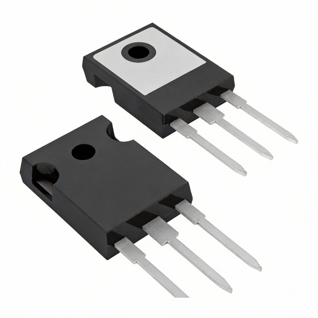 | IPB042N10N3G | Infineon | 4,240 | |
 | IPB042N10N3GATMA1 | Infineon | 6,800 | |
| IPB042N10N3GE8187ATMA1 | Infineon | 1,170 |
No. It is the maximum table value at the specified 10 V gate drive and 100 A test current under the stated table test conditions. Resistance changes with temperature and operating conditions. The temperature plot can inform the loss model, but its labeled curves must retain their statistical or typical meaning.
No. The continuous-current rating is specified with the case at 25°C and subject to the datasheet's operating limits. It does not establish what the assembled PCB, connector, copper, driver, or cooling arrangement can carry. Use the application's RMS current and complete thermal model to determine a workable operating point. Datasheet, Table 2 and Diagram 2.
No. The listing supports considering the device for that class of application. Efficiency depends on the whole converter and operating point; lifetime requires its own thermal, environmental, and reliability validation. This article reports calculations and a proposed evaluation method, not measured efficiency, service life, or YG Group qualification results.
IPB042N10N3G is the compact product-name spelling of Infineon's IPB042N10N3 G, a 100 V N-channel OptiMOS 3 MOSFET in D²PAK. Infineon lists PV power optimizers among its applications. Evaluating it for a PV stage requires checking hot conduction resistance, switching and gate-drive demand, voltage transients, and the complete thermal path. The useful decision is whether those checks close at the intended operating points, not whether one headline current rating looks sufficient. Infineon product record.
A photovoltaic power optimizer is a DC–DC converter that adjusts operation around the panel's maximum power point as conditions change. Infineon's application overview identifies power transistors, gate drivers, sensing, and control as separate elements of that system. A MOSFET application listing establishes relevance to this design task; it does not validate a particular converter, MPPT implementation, or service lifetime. Infineon PV power-optimizer overview.
Before estimating losses, write down the actual voltage and current seen by each switch. Include the panel's maximum cold open-circuit voltage where it reaches that switch, converter topology, duty-cycle range, switching frequency, current ripple, startup, and fault behavior. The drain stress depends on the circuit, so a nominal panel voltage is not a substitute for the maximum VDS waveform.
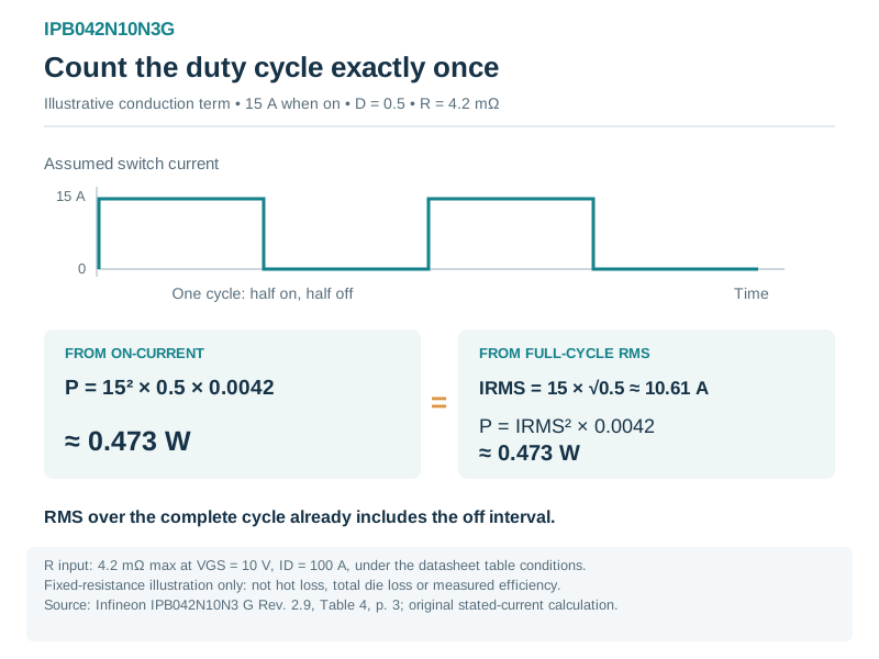
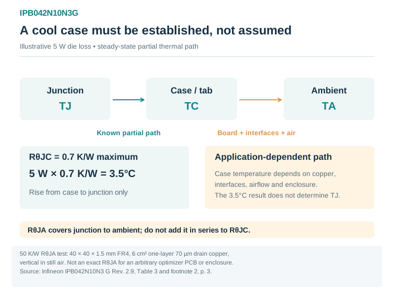
**Figure 1. IPB042N10N3G conduction-loss calculation without double-counting duty cycle.** Illustrative conduction-only calculation: 15 A flows for 50% of each cycle and zero otherwise. Using 4.2 mΩ as the selected resistance input, 15² × 0.5 × 0.0042 and (15√0.5)² × 0.0042 both give approximately 0.473 W. Full-cycle RMS already includes duty. The 4.2 mΩ table maximum is specified at VGS = 10 V and ID = 100 A under the table conditions; this simplified example is not a hot-loss prediction, total MOSFET dissipation or measured efficiency. Sources: [supporting source 1](https://www.infineon.com/assets/row/public/documents/24/49/infineon-ipb042n10n3-g-ds-en.pdf). **Figure 2. IPB042N10N3G junction-to-case rise is only part of the thermal path.** Illustrative steady-state partial-path calculation: 5 W assumed total die dissipation × 0.7 K/W maximum RθJC = 3.5°C junction-to-case rise. This does not determine case or junction temperature relative to ambient. The separate 50 K/W RθJA value describes the datasheet test board and is not a series element to add to RθJC. Board copper, interfaces, airflow and enclosure require application-specific review; no measured or qualified temperature is shown. Sources: [supporting source 1](https://www.infineon.com/assets/row/public/documents/24/49/infineon-ipb042n10n3-g-ds-en.pdf#page=3).IPB042N10N3G is a 100 V class device, not a general-purpose switch for a high-voltage PV string. Its datasheet specifies a minimum breakdown voltage of 100 V at VGS = 0 V and ID = 1 mA. That breakdown test is not a recommended continuous operating point with zero room for overshoot. Establish a design voltage margin from the actual circuit and verify switching transients before accepting the part. Datasheet, Table 4.
The name also needs careful handling in purchasing. The datasheet uses IPB042N10N3 G; the current official product page lists IPB042N10N3GATMA1 as an ordering part number. The article retains IPB042N10N3G as its product identifier. It does not establish the packaging suffix or condition of any particular inventory lot. Verify the full supplier label and purchase documentation separately. Infineon ordering information.
The technical source is Infineon's final datasheet, Rev. 2.9, July 17, 2017. Its tables and curves provide different types of information: guaranteed limits at stated conditions, typical switching behavior, and application-dependent thermal data. Keep those roles distinct.
| Datasheet quantity | Value and condition | What it can support |
|---|---|---|
| RDS(on) | 4.2 mΩ maximum, VGS = 10 V, ID = 100 A | A specified resistance input at that test condition; hot operation needs further treatment |
| RDS(on), lower gate drive | 7.4 mΩ maximum, VGS = 6 V, ID = 50 A | Evidence that the 10 V resistance limit cannot simply be reused at a lower drive voltage |
| Total gate charge Qg | 88 nC typical, 117 nC maximum; VDD = 50 V, ID = 100 A, VGS = 0–10 V | A gate-drive demand estimate at the stated switching condition |
| Gate-drain charge Qgd | 16 nC typical at the same gate-charge condition | Input to evaluating the Miller transition with the actual driver |
| Junction-to-case thermal resistance | 0.7 K/W maximum | Temperature rise from case to junction, not the complete board-to-air path |
| Junction-to-ambient thermal resistance | 50 K/W for the specified 6 cm² copper test arrangement | A reference board condition, not a universal PCB value |
| Junction-temperature limit | 175°C maximum | A limit to respect, not a normal operating target or lifetime guarantee |
Table 1: Inputs for a loss review. Source: Infineon datasheet, Tables 2–6. Compiled by YG Group.
The threshold voltage needs a different interpretation. The 2–3.5 V threshold range is measured at only 150 µA with VDS = VGS. It is not evidence that a 3.3 V logic signal fully enhances the MOSFET at power-stage current. Choose the driver using the intended on-state VGS and its transient behavior, rather than treating threshold as a recommended gate-drive voltage. Datasheet, Table 4.
For a first conduction-loss calculation, use:
Pcond ≈ I²RMS,switch × RDS(on, operating condition)
Here the RMS current is taken over the complete switching period for that particular MOSFET. If it already includes the off interval, do not multiply by duty cycle again. Alternatively, for an idealized flat current I during an on fraction D and zero otherwise, Pcond ≈ I² × D × RDS(on). These are circuit calculations based on resistive dissipation; they are not an Infineon efficiency claim.
Consider a screening example with a flat 15 A during half the cycle. Using 4.2 mΩ as the selected tabulated resistance input gives 15² × 0.5 × 0.0042 = 0.473 W. This does not predict the hot loss of an actual optimizer. It deliberately isolates the conduction term so that the sensitivity to resistance is visible.
| Assumed resistance relative to the 4.2 mΩ input | Resistance used | Calculated conduction loss |
|---|---|---|
| 1.0 × | 4.2 mΩ | 0.473 W |
| 1.5 × | 6.3 mΩ | 0.709 W |
| 2.0 × | 8.4 mΩ | 0.945 W |
Table 2: Illustrative resistance sensitivity at 15 A during 50% of the cycle. Calculation by YG Group using the Table 4 resistance input. The multipliers are assumed sensitivity cases, not specified temperature coefficients or measured results.
The datasheet's resistance-versus-junction-temperature plot shows the direction of the hot-resistance change and separately labels typical and 98% curves. Do not relabel either curve as a guaranteed worst-case production limit at every temperature. Use it to inform a model, document the chosen margin, and validate the model at the intended operating conditions. The current-dependent curves also make clear why a single room-temperature number cannot describe every gate voltage and current. Datasheet, Diagrams 6 and 9.
For a real optimizer, repeat the calculation at operating points that produce different current and duty cycle. A maximum-output-power point is useful, but it need not be the point with the highest RMS current in every switch. Current ripple and the topology determine which device experiences the larger conduction burden.
The gate-charge table supports an approximate gate-drive energy calculation. Charging the gate through a 10 V swing at 100 kHz, using the datasheet's 88 nC typical charge, gives:
Pgate ≈ Qg × Vdrive × fsw = 88 nC × 10 V × 100 kHz = 0.088 W
At 200 kHz, the same input gives 0.176 W. Using the 117 nC maximum table value instead gives 0.117 W at 100 kHz under that charge-test condition. These estimates describe energy drawn for gate charging. They are not all heat dissipated in the MOSFET die: the driver, external gate resistance, and internal gate resistance share dissipation. Nor do they include the drain's turn-on and turn-off switching energy. Datasheet, Table 6 and gate-charge waveform.
Peak drive capability is a separate check from average supply current. During the Miller interval, the available source/sink current and gate-loop impedance influence how quickly VDS changes. The datasheet's 16 nC typical Qgd and gate-charge curve give starting information, but the actual driver output impedance, external resistor, layout, and operating voltage remain part of the circuit.
Do not calculate converter switching loss by blindly inserting the table's rise and fall times into every operating point. The published typical times use VDD = 50 V, VGS = 10 V, ID = 50 A, and RG = 1.6 Ω. A different driver or layout can produce different transitions, overshoot, and ringing. Datasheet, Table 5.
For an engineering evaluation, estimate or measure the turn-on and turn-off energy for the actual commutation, then use Psw = (Eon + Eoff) × fsw within the defined energy-accounting convention. If those measured energies already include output-capacitance and diode-recovery effects, adding those effects again would double-count them. Record what each energy term includes.
In a synchronous power stage, gate timing determines how much of the commutation interval uses the MOSFET channel and how much uses its body diode. The datasheet provides diode forward characteristics and reverse-recovery data, but those are tied to their stated current, voltage, temperature, and current-slew conditions. They do not establish a fixed loss per transition for every PV converter. Datasheet, Table 7 and Diagram 12.
Check dead time across the control and driver tolerances. Excessive diode conduction can add loss; shortening dead time without checking switching overlap can introduce a different problem. This is why the proposed validation captures both gate-source waveforms together with the switching node, rather than judging the stage from a single low-side gate trace.
Output capacitance also varies with drain voltage. The datasheet gives Coss at one test voltage and plots its variation in Diagram 11. Multiplying that single-point capacitance by a voltage-squared formula is only a simplified model; it is not a complete voltage-dependent energy characterization. Use a suitable device model or measured commutation energy when that term materially affects the decision. Datasheet, Table 5 and Diagram 11.
D²PAK is the physical route from silicon to the board's thermal structure, not a guarantee of a particular ambient power rating. The datasheet identifies gate pin 1, drain pin 2 and tab, and source pin 3. The drain-connected tab therefore has electrical as well as thermal consequences for copper placement and any heatsink arrangement. Datasheet, page 1 and package outline.
The 0.7 K/W maximum junction-to-case value can estimate only that section of the heat path. For an illustrative total die dissipation of 5 W, it gives a 3.5°C junction-to-case rise in a steady thermal model. It says nothing by itself about whether the case can be held at the assumed temperature. The PCB, solder connection, thermal interface, airflow, enclosure, and neighboring heat sources determine the rest.
The 50 K/W junction-to-ambient value has a specific test arrangement: a 40 × 40 × 1.5 mm FR4 board with 6 cm² of one-layer, 70 µm copper at the drain connection, vertical in still air. A compact optimizer board in an enclosure can have a different thermal path. Reusing 50 K/W as an exact value for that board would conceal rather than resolve the thermal uncertainty. Datasheet, Table 3 and footnote 2.
For pulsed heating and startup, review transient thermal impedance and safe operating area with the appropriate pulse duration and repetition. The datasheet's SOA plot is given at TC = 25°C with a single-pulse condition; it should not be read as an unlimited repetitive linear-mode allowance. A favorable on-resistance calculation does not validate prolonged partially enhanced operation. Datasheet, Diagrams 3–4.
IPB027N10N5 and IPB020N10N5 are relevant comparison candidates because Infineon's official records identify them as 100 V N-channel devices in the same D²PAK/PG-TO263-3 package family. That establishes a useful starting set, not electrical equivalence or a drop-in approval. IPB027N10N5 record, IPB020N10N5 record.
A meaningful comparison would hold the converter, driver, gate voltage, frequency, temperature target, and measurement method constant. Compare hot conduction loss, commutation energy, gate-drive demand, diode behavior, and thermal performance. Review the complete current datasheets and package drawings before an engineering substitution. This article does not transfer IPB042N10N3G curves to those other devices or rank them from an unmatched resistance/charge table.
There is also a source discrepancy worth retaining in the design record: the current IPB042N10N3 G webpage shows a different pulsed-current figure from Rev. 2.9 of the datasheet. No pulsed-current number is used here to size the stage. Resolve that particular limit with Infineon if the design depends on it; do not silently choose the larger value.
An IPB042N10N3G evaluation should finish with the operating envelope, waveform-derived current, stated resistance assumptions, switching-energy accounting, gate-drive calculation, and thermal path in one record. Verify the highest-stress conditions on the intended hardware before approving the stage. That makes a lower-loss claim testable and lets the next engineer distinguish a useful comparison from a change that merely improves one datasheet headline.
Author: Alice Chen