
Susanna Feng




| Picture | Part Number | Manufacturer | Stock | Action |
|---|---|---|---|---|
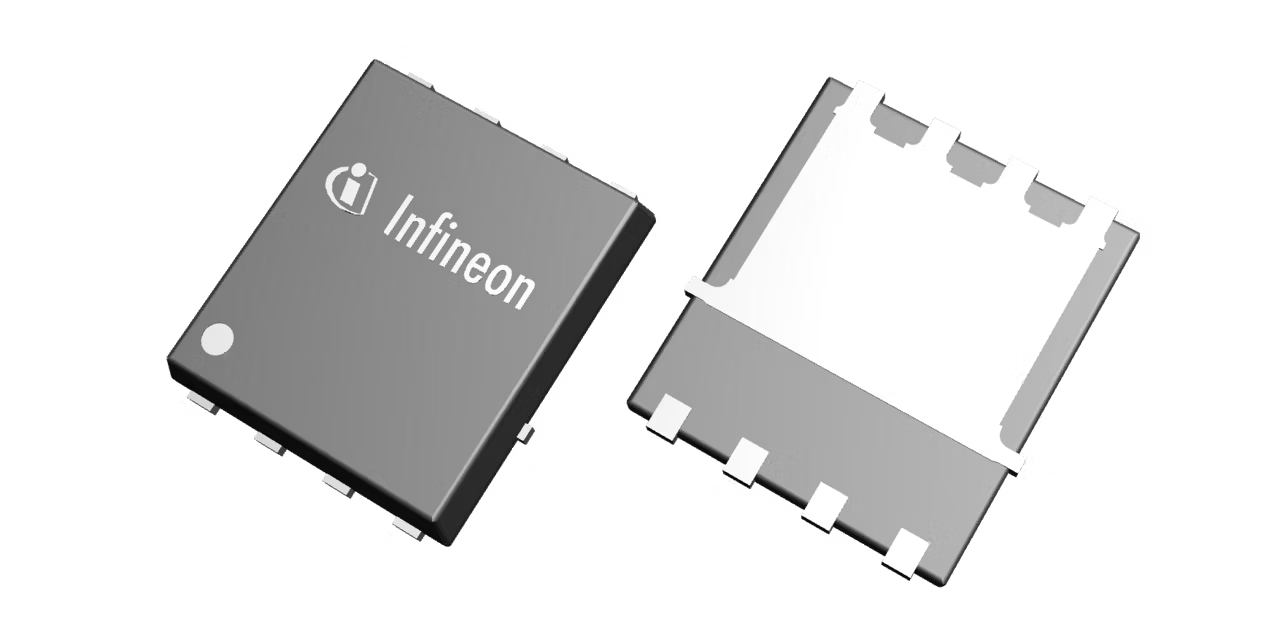 | BSC052N08NS5 | Infineon | 6,840 | |
 | BSC070N10NS3GATMA1 | Infineon | 5,890 |
The inductive term is 15 V, so the first-order result is 69 V. This calculation excludes resonant ringing and clamp dynamics and is not a measured BSC052N08NS5 waveform.
No. It is an illustrative 80% engineering policy. Choose the actual budget from system requirements, tolerances, temperature and validation rather than treating that percentage as a universal rule.
Source pins 1–3 provide the reference. Gate is pin 4; Drain is pins 5–8 plus the exposed pad. The Gate signal is separate from the Source return, and the thermal pad stays on the Drain net.
No. It is specified under particular single-pulse test conditions. Repetitive avalanche requires a separate thermal and reliability assessment; use qualified layout and protection measures to manage the real switching stress.
By Susanna Feng | YG GROUP
BSC052N08NS5 is an 80 V N-channel MOSFET in SuperSO8. On a nominal 48 V rail, the maximum supply and switching overshoot consume its margin; a calculated L × di/dt budget helps identify the required loop and protection checks without predicting a measured waveform.
The datasheet provides an 80 V minimum breakdown specification at its stated 25 °C test condition and a ±20 V gate-source absolute rating. Its 5.2 mΩ maximum on-resistance is specified at 10 V gate drive, 47.5 A drain current and 25 °C junction temperature. Keep those conditions with the figures when comparing candidates. BSC052N08NS5 Rev. 2.1 datasheet.
Use the system specification to establish maximum steady supply, startup behavior and defined surge events. A 54 V or 57 V example can help explain the arithmetic, but neither value is automatically the limit of every 48 V system. Preserve tolerances, charging conditions and the environment in the voltage budget.
An illustrative policy might allocate only 80% of the MOSFET rating to the planned peak stress: 0.8 × 80 V = 64 V. This is a chosen engineering budget, not a universal manufacturer requirement. At a 54 V maximum bus, it leaves 10 V for the modeled overshoot; at 57 V it leaves only 7 V.
Table 1. Illustrative voltage-headroom allocation | Source: manufacturer documents in References; assumptions and operating conditions are stated in the table or adjacent text. Compiled / calculated by: YG GROUP.
| Illustrative case | Bus voltage | Remaining headroom to 64 V |
|---|---|---|
| Example A | 54 V | 10 V |
| Example B | 57 V | 7 V |
| Rating reference | 80 V | Absolute-rating comparison, not a design target |
The selected policy also needs temperature and tolerance reasoning. Typical breakdown-versus-temperature curves describe behavior under their test conditions; they should not be extrapolated into a guaranteed cold-temperature limit with an invented fixed coefficient. Evaluate the required environmental range with applicable manufacturer guidance and system validation.
A first-order voltage estimate is Vpeak ≈ Vbus + Lloop × |di/dt|. With inductance in nH and slew in A/ns, their product is directly in volts. Thus 5 nH at 3 A/ns contributes 15 V. Adding that to a 54 V bus gives 69 V, not 63 V.

Figure 1. First-order calculations at 3 A/ns. The graph excludes resonant ringing, clamp dynamics and temperature-dependent device behavior. Source: manufacturer documents in References; calculation / diagram: YG GROUP.
At that same slew, meeting the illustrative 64 V budget would require Lloop no greater than about 3.33 nH for a 54 V bus or 2.33 nH for a 57 V bus. These figures expose how quickly the headroom is consumed. They are not extracted PCB inductances or measured drain waveforms.
Actual commutation includes nonlinear capacitances and distributed parasitics. The simple equation helps establish an initial constraint, but it cannot predict ringing amplitude or a clamp's dynamic response. Use measurement and an appropriate model to examine the real circuit, including the probe connection and its influence on the observed waveform.
In a half-bridge, place the local input capacitor to minimize the high-frequency commutation loop through the switches and return. Keep the relevant connections compact and avoid unnecessary loop area. The most useful geometry depends on the actual layer stack and current path; a universal number of vias or a generic trace-width recipe cannot establish its inductance.
The SuperSO8 pin map is Source 1–3, Gate 4 and Drain 5–8 plus the exposed Drain pad. The pad therefore belongs to the Drain net, even when copper area is added for cooling. It must not be renamed ground solely because it is a thermal surface.

Figure 2. Illustrative half-bridge with BSC052N08NS5 in the low-side position. The Gate signal and the separate Source return are shown explicitly; the series RC snubber spans Drain and Source. Source: manufacturer documents in References; calculation / diagram: YG GROUP.
Reference the driver's return to the MOSFET Source connection rather than a remote power-ground point with shared switching impedance. This reduces unwanted source-voltage feedback into the gate drive. The gate trace itself is not a Kelvin return; the return is the Source-reference path used by the driver.
A series RC snubber across Drain and Source can damp a resonance when selected for that circuit. Determine the relevant ringing frequency and energy, evaluate dissipation, and verify its effect at the demanding switching conditions. A nominal resistor/capacitor pair does not guarantee a fixed reduction in peak voltage on another layout.
Likewise, a transient suppressor must be evaluated at the actual current, temperature and wiring inductance. Standoff voltage alone is insufficient; its clamping voltage can consume the available MOSFET margin. Keep normal operating voltage, surge voltage, clamp characteristics and MOSFET limits in the same review rather than promising protection from a family-level TVS label.
The datasheet's single-pulse avalanche specification uses defined current, gate resistance and starting junction temperature. It does not authorize arbitrary repetitive avalanche in a converter. Account for repetition, temperature rise and reliability requirements through the applicable qualification process rather than treating the energy figure as a continuous protection allowance.
Table 2. Related MOSFET voltage-rating comparison | Source: manufacturer documents in References; assumptions and operating conditions are stated in the table or adjacent text. Compiled / calculated by: YG GROUP.
| Model | Manufacturer-supported distinction | Review requirement |
|---|---|---|
| BSC052N08NS5 | 80 V N-channel SuperSO8 | Actual VDS/VGS stress and thermal operating point |
| BSC070N10NS3GATMA1 | 100 V SuperSO8 candidate | Gate charge, losses, footprint and transient qualification |
The Infineon BSC070N10NS3 G product page identifies a concrete 100 V candidate. Greater blocking voltage can improve the available budget, but it does not automatically improve efficiency or make the device interchangeable. Compare resistance and charge at compatible test conditions before making a switching-loss claim.
For the released board, measure drain-source voltage with a suitable differential setup and measure gate-source voltage at the package reference. Exercise the specified rail, load, temperature and transition conditions, including startup and faults. Retain the protection network, gate resistance and layout revision with the result so the margin assessment applies to the assembly that will actually be built.