
Doris Lee



6 views

| Picture | Part Number | Manufacturer | Stock | Action |
|---|---|---|---|---|
 | AT45DB641E-SHN2B-T | Renesas | 2,280 | |
| AT45DB641E-SHN-T | Renesas | 6,600 |
The family offers that standard configuration, but the exact 2B ordering option is specifically listed for 256-byte binary pages. Read the actual status during integration and receiving tests because configuration can subsequently be changed and retained.
For AT45DB641E, Revision O describes the setting as reversible. It persists across power cycles and has a 10,000-cycle configuration-register limit. Do not assume that rules from a different DataFlash generation apply to this device.
The cited datasheet describes them as user-accessible storage. Any proposed header, sequence number, checksum or recovery format in those bytes must be defined and validated by the application.
Binary addressing can simplify one part of a driver, but it does not qualify its commands, buffer behavior, erase geometry, protection handling or power-failure recovery. Validate those paths for AT45DB641E explicitly.
By Doris Lee
AT45DB641E-SHN2B-T is a Renesas DataFlash ordering code supplied with a 256-byte binary page configuration. That makes its page addressing different from the 264-byte configuration associated with AT45DB641E-SHN-T. For an embedded design, the choice affects address construction, stored-record layout, programming tools and replacement approval. The useful starting point is to align the ordered variant, the device's actual configuration and the firmware's assumptions before moving data into production.
Renesas explicitly lists both ordering codes in its AT45DB641E datasheet. In the ordering diagram, 2B means the binary 256-byte page option; the absence of that option means the standard 264-byte page option. The final T identifies tape-and-reel shipment. Both listed SHN variants use the 8-lead, 208-mil-wide SOIC package. These are separate fields with separate consequences: shipment format does not explain page organization, and package similarity does not establish firmware compatibility. Renesas datasheet, section 28, page 74.
A BOM that retains AT45DB641E-SHN2B-T therefore communicates more than a memory family and density. It tells purchasing which factory page configuration the software team expects. A programmer configuration or receiving document that truncates the code to AT45DB641E removes that distinction.
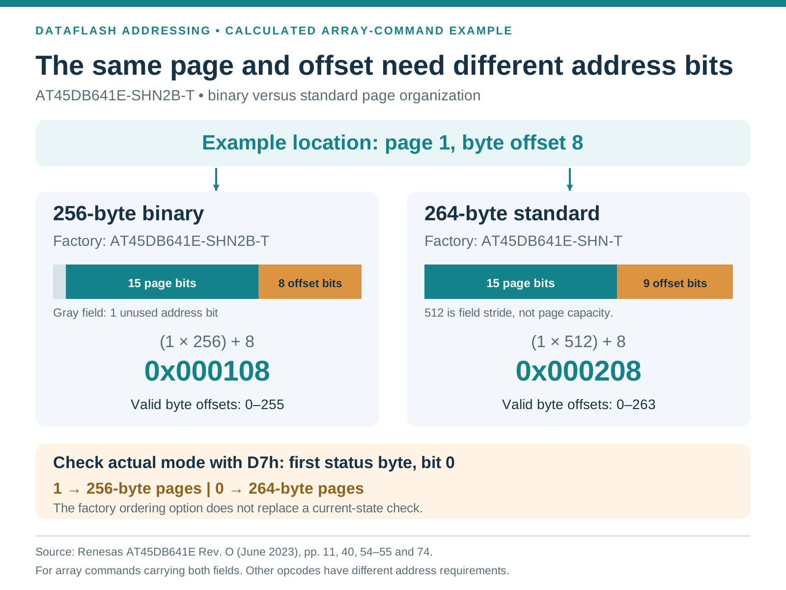
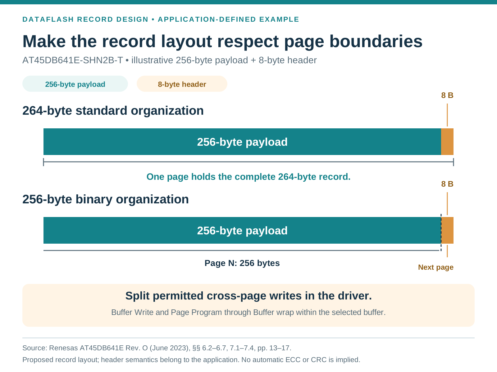
**Figure 1. The same page and offset need different address bits.** Address construction for the same logical page and byte offset under the two AT45DB641E organizations. Binary mode uses an eight-bit offset field; standard mode uses nine bits, but only offsets 0–263 contain page data. The formulas apply to array commands carrying both fields, not every opcode. Check the first status byte’s page-size bit; the factory option is not proof of current state. Sources: [supporting source 1](https://www.renesas.com/en/document/dst/at45db641e-datasheet). **Figure 2. Make the record layout respect page boundaries.** Illustrative record packing at a page start: a 256-byte payload plus an application-defined eight-byte header fits one 264-byte standard page but spans binary pages. Both lanes use the same byte scale. The driver must deliberately split allowed cross-page writes or reject them; Buffer Write and Main Memory Page Program through Buffer wrap within the selected buffer. The header does not imply chip-provided ECC, CRC or recovery semantics. Sources: [supporting source 1](https://www.renesas.com/en/document/dst/at45db641e-datasheet).The ordered option is also different from the current state of a particular device. Renesas makes the page-size setting reversible and stores it in a nonvolatile register. A previously configured component can consequently retain a setting across power cycles. Read the page-size status bit during controlled initialization; do not assume that a familiar label is a substitute for checking the state that the driver will use. Datasheet, sections 10.4 and 12, pages 40–47.
The array contains 32,768 pages. Each page can expose 256 or 264 bytes, and the two SRAM buffers follow the selected size. The extra eight bytes in standard mode are user-accessible storage, rather than an automatic promise that the memory will maintain an application's checksum, timestamp or record header. Their purpose is a software design decision. Datasheet, sections 1 and 12, pages 6 and 47.
| Decision field | Binary page configuration | Standard DataFlash page configuration |
|---|---|---|
| Page and buffer size | 256 bytes | 264 bytes |
| Number of pages | 32,768 | 32,768 |
| Total accessible array bytes, calculated | 8,388,608 bytes, or 8 MiB | 8,650,752 bytes, or 8.25 MiB |
| Within-page address field | 8 bits | 9 bits, with valid byte offsets 0–263 |
| Page-size status indication | First status byte, bit 0 = 1 | First status byte, bit 0 = 0 |
| Relevant factory-configured order code | AT45DB641E-SHN2B-T | AT45DB641E-SHN-T |
Table 1: Page-organization comparison. Source: Renesas datasheet, pages 6, 11, 40, 47 and 74. Byte totals are calculated from the documented page count and size; MiB means 1,048,576 bytes. Compiled by YG Group.
The standard organization adds 262,144 accessible bytes in total. That is a useful amount of space when a record already consists of 256 payload bytes plus eight bytes of application-managed metadata. It is less attractive when all firmware, file-format and programming assumptions are built around power-of-two pages and the extra space would remain unused.
Neither choice creates a general SPI NOR replacement. DataFlash commands, buffer use, erase operations, busy handling and protection behavior still need explicit driver support. Selecting a convenient page size solves one part of the integration problem.
The command interface uses three address bytes, but the interpretation of those bytes changes with the page configuration. In binary mode, the main-memory address uses 15 page bits and eight byte-offset bits, with an additional unused bit in the three-byte transfer. In standard mode, it uses 15 page bits and nine byte-offset bits. Renesas describes this in section 5 and provides command-specific layouts in Tables 32 and 33. Datasheet, pages 11 and 54–55.
For an array command that accepts both a page and a byte offset, the following arithmetic expresses the field placement:
The second expression uses 512 because a nine-bit field is reserved for the offset. It does not mean that 512 bytes are available in each page. In standard mode, offsets 264–511 are outside the documented page payload. A driver should reject an invalid offset instead of treating the unused encoded range as additional memory.
Consider page 1, byte offset 8. Its encoded array address is 0x000108 in binary mode and 0x000208 in standard mode. The logical location has the same page and offset, but the command bytes differ. A driver that changes only its page-length constant while retaining the old address shift can therefore access a different location.
A second example exposes a particularly easy test gap. Encoded address 0x000100 identifies page 1, byte 0 in binary mode; in standard mode, the same bits identify page 0, byte 256. Reading and writing only the first 256 bytes of page 0 can leave this mistake undetected. Boundary tests must reach beyond that region.
These examples apply to commands with both address fields. They are not universal byte sequences for every instruction. Buffer-only commands, page erase, block erase and page-to-buffer transfers have their own required and unused bits. Use the row for the actual opcode in the command table, and transmit the most significant bit first as specified. A reusable address helper should make the command type and page configuration explicit rather than silently applying one formula to every operation.
There is also a documentation detail worth checking when porting old code: some later waveform annotations in Revision O show buffer-address widths inconsistent with section 5, section 6.7 and the dedicated addressing tables. For the page-organization explanation here, those consistent sections and Tables 32–33 are the basis. Do not copy a contradictory waveform label into a driver; obtain manufacturer clarification where the implementation depends on it.
Page size is most useful when considered alongside the application's record structure. A stream of bytes, a fixed record and an updateable configuration object place different demands on the memory driver.
For a proposed 256-byte payload plus eight-byte header, standard mode can place the complete 264-byte record in one page. The header could hold a sequence counter and application-defined integrity information, provided the software defines their format and recovery behavior. This is an architectural example, not a feature automatically implemented by the chip.
In binary mode, the same 264-byte record spans pages unless the application changes its layout. One possible approach is to separate payload pages from an index area; another is to use a smaller payload so that all record fields fit in 256 bytes. Each approach changes capacity accounting and recovery rules. Choose deliberately rather than letting a generic write function decide by wrapping data.
The datasheet describes wrap behavior that matters here. A Buffer Write reaching the end of a buffer wraps to its beginning. The Main Memory Page Program through Buffer command also wraps within its selected buffer when more data are clocked in. A Continuous Array Read can cross into the next page, whereas a Main Memory Page Read wraps within the same page. Those operations are not interchangeable implementations of a generic “read or write N bytes” API. Datasheet, sections 6.2–6.7 and 7.1–7.4, pages 13–17.
A practical driver contract should specify whether a request may cross a page boundary. If it may, the driver must split the request into the appropriate operations. If it may not, the driver should return a clear error before issuing an oversized transaction. Silent wrapping is particularly difficult to diagnose because the transaction can complete while earlier buffer positions have been overwritten.
The Status Register Read opcode is D7h. The first returned status byte carries PAGE SIZE in bit 0: one indicates 256-byte pages, and zero indicates 264-byte pages. The register returns two bytes, then repeats that two-byte sequence while clocks continue. A polling loop must preserve the byte position; bit 0 of the second byte describes erase-suspend state, not page size. Datasheet, Tables 20–21, pages 40–41.
This gives production software a straightforward check: compare the observed page configuration with the configuration recorded for the image and driver. If they differ, stop normal programming and route the unit through an intentional configuration procedure. Automatically changing the mode on every boot conceals mismatches and needlessly writes the nonvolatile configuration register.
Renesas documents these page-size command sequences:
| Intended configuration | Four command bytes, hexadecimal | Completion requirement |
|---|---|---|
| 256-byte binary pages | 3D 2A 80 A6 | Deassert CS, allow the internal configuration cycle to finish, then verify the status |
| 264-byte standard pages | 3D 2A 80 A7 | Deassert CS, allow the internal configuration cycle to finish, then verify the status |
Table 2: Page-configuration commands. Source: Renesas datasheet, section 12 and Table 22, page 47. These are configuration instructions, not a complete data-migration routine. Compiled by YG Group.
The setting takes effect after the internal process completes; a power cycle is not required. The register has a specified limit of 10,000 erase/program cycles. Treat a mode change as a controlled configuration event, rather than an ordinary per-record operation.
Changing the organization is also not evidence that an existing image has been converted to a new logical layout. Before a planned change on populated memory, preserve the data in a known format, record its original organization and define how it will be reconstructed and verified. Test the procedure on expendable development units before it becomes part of manufacturing or service tooling. The manufacturer documents the mode commands; the application owns the migration policy.
The two buffers allow software to overlap selected buffer activity with internal array operations, subject to the operation-mode rules. While an allowed array operation uses one buffer, the other can accept the next data block. This can reduce host waiting during transfer, but it does not remove the array's erase/program time. Datasheet, sections 1 and 15, pages 6 and 51.
For example, Revision O lists a maximum page erase-and-program time of 35 ms for either page size over the stated supply ranges. Dividing a 256-byte payload by 35 ms gives approximately 7,314 bytes per second. This is a simple calculation for a page-at-a-time path that erases and programs each page; it excludes bus overhead, scheduling delays, verification and recovery. It is not a measured sustained write rate or a guarantee for the complete system. Datasheet, section 19.5, page 61.
The useful design question is whether the application can buffer its incoming data while the selected operation finishes under its required conditions. A headline SPI clock frequency does not answer that question. Also check supply-dependent frequency limits: the detailed AC table distinguishes the 1.7–3.6 V and 2.3–3.6 V ranges and different read opcodes. Do not apply the ordering table's 85 MHz summary to every command at every supply voltage. Datasheet, section 19.4, page 60.
For long-lived logging, record layout and write distribution belong in the same review. The datasheet's Auto Page Rewrite discussion requires attention when static pages share a sector with pages that undergo many erase/program operations: it calls for each page to be updated or rewritten within 50,000 cumulative page erase/program operations in that sector. A design that repeatedly updates one small metadata record should review this requirement instead of relying only on the headline per-page endurance figure. Datasheet, section 10.3 and Figure 52, pages 39 and 73.
AT45DB641E-SHN-T is a useful comparison because it isolates the page-option distinction within the same listed package family. It is not an automatically approved substitute for AT45DB641E-SHN2B-T. Any proposed substitution should identify who owns the configuration step and whether the existing programming tool, image format, boot path and service tools recognize the resulting organization.
A focused acceptance test should produce a record that another engineer can reproduce:
This is a proposed engineering acceptance sequence, not a report of testing performed by YG Group. The electrical identity command is documented in section 13; its returned identification fields do not encode every commercial attribute of the complete ordering code. Likewise, a ready indication alone is not proof that the intended data reached the intended address. Check operation results and read back the required data. The EPE error bit does not report every aborted operation, including attempts against protected regions. Datasheet, pages 42 and 48–49.
AT45DB641E-SHN2B-T is a clear choice when the approved design expects factory-configured 256-byte pages. The important follow-through is to preserve that expectation in the BOM, address helpers, programmer job, image format and acceptance record. Standard 264-byte mode can be useful when the application intentionally uses its additional bytes, but switching modes requires a deliberate software and data-layout decision. Keeping those decisions aligned is what turns a suffix check into a reliable embedded-memory selection.