
Eyki Chen




| Picture | Part Number | Manufacturer | Stock | Action |
|---|---|---|---|---|
 | AD8221ARMZ-R7 | Analog Devices | 5,710 | |
 | AD8220ARMZ-R7 | Analog Devices | 5,580 | |
| AD8226ARMZ-R7 | Analog Devices | 8,490 | |
 | AD8421ARMZ-R7 | Analog Devices | 5,870 | |
| AD8422ARMZ-R7 | Analog Devices | 7,180 |
Yes, the AD8221 datasheet includes a 5 V strain-gauge application with a 2.5 V reference. That supports the basic circuit arrangement, but the usable signal span still depends on gain, bridge common-mode voltage, output loading, and temperature. The amplifier is not a rail-to-rail-output device. Calculate the largest required output excursion, including bridge imbalance and excitation tolerance, and check the internal operating region as well as the output swing. Do not apply offset limits specified at ±5 V to ±15 V directly to a single-5 V design without applicable evidence. See Analog Devices' AD8221 Rev. C datasheet, Table 2 and the strain-gauge application.
Multiply sensitivity by excitation first. An assumed 2 mV/V bridge with 5 V excitation produces 10 mV at nominal full scale. AD8221 uses G = 1 + 49.4 kΩ/RG, so 499 Ω gives approximately 100 gain. At VREF = 2.5 V, an assumed differential input of ±10 mV would ideally produce approximately 1.5 V to 3.5 V. Those values are arithmetic, not a verified operating range. Add sensor zero-balance error, overload requirements, resistor tolerance, and reference uncertainty before accepting the gain. Check common-mode and output headroom at the resulting endpoints.
AD8221ARMZ-R7 uses the ARM table, which specifies 70 µV maximum input offset under the stated room-temperature and ±5 V to ±15 V supply conditions. The 25 µV headline applies to the BR grade. Its drift and other limits also need the ARM entries. The specified performance range is −40°C to +85°C; operation to +125°C does not extend every guarantee. Keeping the exact grade in the error budget prevents calibration and temperature allowances from being based on a different ordering model.
By Eyki Chen
AD8221ARMZ-R7 is an Analog Devices instrumentation amplifier worth considering when a bridge sensor produces a small differential signal riding on a much larger common-mode voltage. Selection starts with the ARM-grade limits, the bridge's maximum imbalance, and the amplifier's available input and output headroom. A gain calculation alone cannot establish that the circuit will stay linear. A useful bridge front end must preserve the small signal through amplification, filtering, and conversion without losing valid measurements to clipping.
The ordering table in the AD8221 Rev. C datasheet identifies AD8221ARMZ-R7 as an eight-lead MSOP device supplied on a seven-inch tape-and-reel. Its specified temperature range is −40°C to +85°C. The separate operational range extends to +125°C, but that statement does not extend every electrical guarantee to that temperature. An outdoor measurement system should therefore compare its required guaranteed range with the specification tables, rather than treating the wider operational range as an interchangeable rating.
The grade distinction matters even at room temperature. The prominent 25 µV input-offset figure on the datasheet's first page belongs to the BR grade. For ARM devices, Table 2 gives a 70 µV maximum input offset under its stated supply conditions. The ARM input-offset drift limit is also different. Carrying a better-grade headline into an ARM bill of materials can leave the design's calibration allowance too small before the first board is built.
*Figure 1. Conceptual bridge-conditioning path for AD8221ARMZ-R7. The assumed 5 V excitation and 2.5 V reference illustrate the review; the diagram is not a validated schematic or a measured transfer curve.* *Figure 2. A proposed diagnostic sequence for an AD8221ARMZ-R7 bridge front end. Each step isolates a different failure mechanism; no bench results or pass rates are implied.*A divider is not automatically adequate simply because its unloaded voltage is correct. AD8221 requires a low-impedance reference drive to preserve performance, and the REF pin is connected into the output difference-amplifier network. Evaluate source impedance, reference current, accuracy, noise, startup, and buffer stability if a buffer is used. Reference error shifts the output directly. Also check the input operating region separately: changing REF cannot recover linear operation when the input stage is already saturated. The manufacturer's reference-terminal discussion is on page 19 of Rev. C.
No. More converter bits do not recover a signal clipped by the amplifier, remove analog offset drift, or establish low-frequency noise performance. A stable initial offset may be calibrated, but its later temperature or time dependence remains part of the budget. Evaluate noise over the actual analog and digital bandwidth, and review the ADC's acquisition requirements and dynamic input load. A converter may need an additional driver or an interface network. Validate the complete sampled signal path rather than inferring usable resolution from the ADC bit count alone.
Four useful candidates are AD8220ARMZ-R7, AD8226ARMZ-R7, AD8421ARMZ-R7, and AD8422ARMZ-R7. Their respective families offer reasons to investigate JFET input behavior, a wider low-voltage supply range, higher-speed precision operation, or rail-to-rail output with low-power operation. These are comparison directions supported by Analog Devices' product pages, not direct-replacement approvals. For each exact model, verify the grade limits, gain equation, pinout, footprint, input and output range, reference behavior, temperature, and converter interface before changing the bill of materials.
AD8221 uses one external resistor to set gain. That keeps the basic circuit compact, but it does not make the surrounding circuit irrelevant. Source resistance affects bias-current error; a reference connection affects output accuracy; and the resistor's tolerance contributes directly to span error. Those are system choices, not defects that disappear because the amplifier contains accurately matched internal resistors.
Table 1. AD8221ARMZ-R7 facts that define the starting point.
| Parameter | Value or identity | Conditions and selection meaning | Source |
|---|---|---|---|
| Package and shipment | Eight-lead MSOP, RM-8; seven-inch tape-and-reel | Exact AD8221ARMZ-R7 ordering entry; packaging suffix does not select BR performance | Rev. C, p. 24 |
| Specified temperature | −40°C to +85°C | Separate from operation to +125°C | Rev. C, pp. 5–7, 24 |
| Supply range | ±2.3 V to ±18 V | Input and output headroom must still be satisfied | Rev. C, Table 2 |
| Gain range | Unity to 1000 | One external resistor; unity gain with the resistor omitted | Rev. C, pp. 17–18 |
| Input offset | 70 µV maximum | ARM grade; supplies from ±5 V to ±15 V; room-temperature table conditions | Rev. C, Table 2 |
| Input offset drift | 0.9 µV/°C maximum | ARM-grade average temperature coefficient | Rev. C, Table 2 |
| Input voltage noise | 8 nV/√Hz maximum at 1 kHz | Spectral density, not integrated bridge measurement noise | Rev. C, Table 2 |
For a slowly changing load cell, offset stability, low-frequency noise, usable output span, and interference rejection usually deserve attention before an impressive small-signal bandwidth number.
Write down the actual measurement task before selecting the gain resistor. Include sensor sensitivity, excitation tolerance, zero-balance tolerance, expected overload, source resistance, cable length, required update rate, and the converter input range. A bridge whose nominal output fits comfortably can still clip during mechanical overload or temperature-induced zero shift. Keeping those cases separate helps distinguish useful measurement range from a recoverable fault condition.
A bridge sensitivity expressed in millivolts per volt must be multiplied by its excitation voltage. Consider an illustrative sensor rated at 2 mV/V with 5 V excitation. Its nominal full-scale differential output is 10 mV. This is an assumed sensor for calculation, not a measured sensor or an AD8221 performance claim. A bipolar force measurement could require a differential span from −10 mV to +10 mV; a unidirectional measurement might use zero to +10 mV.
For AD8221, the nominal transfer relationship is VOUT = VREF + G × (VIN+ − VIN−), with G = 1 + 49.4 kΩ/RG. A 499 Ω resistor gives a nominal gain very close to 100. With VREF at 2.5 V, a ±10 mV differential input therefore maps arithmetically to approximately 1.5 V through 3.5 V. The calculation says where the output would be if the amplifier remains linear. It does not prove that the internal stages can support every required common-mode and output combination.
The distinction becomes obvious when gain is increased. More gain uses more converter codes for the same sensor signal, but also amplifies bridge imbalance and input offset. It reduces the differential input span available before clipping. If an application needs to tolerate a large zero-balance error, using nearly the entire output range for nominal full scale is a poor starting point.
Table 2. Calculated gain choices for an assumed ±10 mV bridge signal.
| External RG | Nominal calculated gain | Ideal output with VREF = 2.5 V | Engineering interpretation |
|---|---|---|---|
| 1.00 kΩ | 50.4 | 1.996 V to 3.004 V | Smaller output span leaves more arithmetic allowance for imbalance |
| 499 Ω | Approximately 100 | Approximately 1.500 V to 3.500 V | Useful starting example, subject to common-mode and swing checks |
| 249 Ω | Approximately 199.4 | Approximately 0.506 V to 4.494 V | Demands output levels too close to the rails for the illustrated 5 V supply arrangement |
Source: nominal gain equation in AD8221 Rev. C, pp. 17–18. Outputs are calculations from an assumed sensor; resistor tolerance, amplifier errors, loading, temperature, and saturation are excluded.
A practical gain worksheet should contain more than the nominal sensor endpoints. Add the maximum positive and negative zero offset specified by the sensor, the largest valid load, and the chosen overload allowance. Apply excitation tolerance to the sensor response if the measurement is not ratiometric. Then calculate the required output endpoints at the reference-voltage extremes. This exposes the worst case directly instead of relying on the assumption that several tolerances will cancel.
Resistor selection belongs in the same worksheet. A close nominal value can be preferable to an exact calculated value if the available resistor has better tolerance and temperature behavior. Calibration can correct an initial slope error within the linear region, but it cannot recover information lost to clipping. Nor can a room-temperature calibration remove every later change caused by the gain resistor, sensor, excitation source, and amplifier drifting differently.
The bridge excitation and the ADC reference also need a deliberate relationship. A ratiometric measurement can reduce sensitivity to excitation variation when the sensor response and conversion scale track the same source appropriately. That is a system-level possibility, not an automatic property of inserting AD8221. Confirm the actual converter reference path, wiring drops, reference loading, and any reference filtering before relying on cancellation.
The bridge common-mode voltage is the average of the two input voltages. A balanced bridge excited between ground and 5 V will often place both sense nodes near mid-supply, while their difference remains only millivolts. That combination is a natural reason to consider an instrumentation amplifier. It still needs checking at the real sensor's resistance extremes, across excitation tolerance, and when faults change one input independently.
AD8221 has internal amplifier stages whose swing requirements depend on differential input, gain, common-mode voltage, and output level. An output voltage inside the supply rails is therefore necessary but insufficient. The datasheet's common-mode-versus-output plots illustrate this coupled boundary. They are typical plots for stated gains, supplies, and temperature; they should not be turned into a universal rectangular input window or treated as guaranteed limits for an unrelated circuit.
The input operating-range rows need equal care. Their footnote specifies one input grounded at unity gain. Quoting that row as the allowable common-mode range at gain 100 discards the condition that makes the number meaningful. When reviewing a bridge design, keep the gain, input common-mode range, reference voltage, and required output span together on one page.
Table 3. Headroom checks before accepting the gain calculation.
| Check | What must be established | Evidence and boundary |
|---|---|---|
| Both input voltages | Each sense node remains within the applicable operating region | Rev. C, Table 2; input-range footnote is a unity-gain condition |
| Common mode versus output | All required operating points fit the selected gain and supply arrangement | Rev. C, Figures 8 and 9 are typical illustrations, not universal guarantees |
| Output loading | Required swing is supported with the actual resistive and dynamic load | Rev. C, Table 2 output-swing rows use a 10 kΩ load |
| Reference drive | Reference voltage remains accurate with a low source impedance | Rev. C, pp. 18–19; REF is part of the output difference-amplifier network |
| Temperature corners | The design retains margin under the applicable over-temperature limits | Rev. C, ARM Table 2; operational range and specified range differ |
At the lower supply range, the ARM table's room-temperature output-swing limits leave headroom from both rails with a 10 kΩ load. The over-temperature rows require different allowances. This amplifier is not a rail-to-rail-output part. A design that assumes it can deliver almost zero to almost 5 V simply because it is powered from 5 V has skipped a material limitation.
The datasheet includes a strain-gauge application using a 5 V supply and a 2.5 V reference. That supports the circuit concept; it does not certify every bridge, gain, ADC, or output span connected in that arrangement. Use the example to understand the signal path, then review the chosen operating points against the electrical conditions. If the available headroom is tight, reducing gain, changing the reference level, or using a different supply arrangement may be more effective than adjusting software scaling.
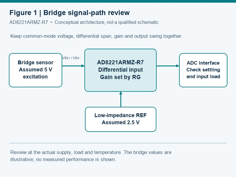
Check the REF source impedance as well as its voltage, because reference error appears directly at the output. A resistor divider may produce the right voltage with no load and still disturb the amplifier's accuracy when connected. Examine the divider's source impedance, the required reference current, and any buffer's stability and startup behavior. Moving REF can shift the output operating point, but it cannot repair an input stage that is already outside its linear region.
Ground references matter especially with remote sensors. The bridge return at the far end of a cable may differ from the local analog ground because excitation current flows through finite wire resistance. That shift changes the sense-node common mode seen by the amplifier. Measure or calculate the relevant voltages at the amplifier pins; a nominally correct excitation voltage measured at the supply connector does not establish the pin conditions.
Offset is best considered in input-referred terms when comparing it with a millivolt bridge signal. AD8221 has input and output offset contributions. At gain G, a simple conservative arithmetic combination is input offset plus output offset divided by G. The quantities must come from the same grade and compatible test conditions. They should not mix a typical plot, a maximum table entry, and a better-grade headline.
For the ARM grade at the stated room-temperature conditions, 70 µV input offset and 600 µV output offset produce an input-referred arithmetic envelope of approximately 76 µV at gain 100. Relative to an assumed 10 mV full-scale signal, that is 0.76%. This is an illustration of the amplifier offset contribution before calibration. It is not a complete system accuracy specification, and these offset limits are specified at supplies from ±5 V to ±15 V, not a guarantee for the earlier single-5 V illustration.
Table 4. Error-budget items that need separate treatment.
| Error term | How it enters a bridge measurement | Treatment and evidence boundary |
|---|---|---|
| Amplifier offset | Input offset plus output offset divided by gain | ARM maxima support the 76 µV example only under their stated supply and temperature conditions; Rev. C, Table 2 |
| Gain uncertainty | Amplifier gain error combines with RG tolerance | Budget initial span error and temperature change separately; Rev. C, pp. 5, 18 |
| Bias current | Source resistance and imbalance create additional input error | ARM room-temperature bias current is 2 nA maximum under the table conditions; Rev. C, Table 2 |
| Low-frequency noise | Changes the short-term stability of a slowly sampled reading | Use the relevant gain and bandwidth; peak-to-peak and spectral-density values are different quantities |
| Sensor and reference errors | Bridge balance, sensitivity, excitation, and reference affect the conversion | Obtain sensor and reference specifications; no complete sensor accuracy is inferred from the amplifier datasheet |
A zero calibration can remove a stable initial offset at the calibration point. A span calibration can correct a stable slope error. Their usefulness depends on what happens afterward: temperature changes, sensor creep, reference drift, mechanical installation, and time all deserve attention. A calibration stored in firmware should include enough context to distinguish a changed sensor from a failed analog front end.
Noise needs a bandwidth definition before it becomes a useful comparison. The 1 kHz voltage-noise density is not the peak-to-peak variation of a slow weighing display. The datasheet separately gives low-frequency noise and gain-dependent frequency-response information. Integrating noise over the actual analog and digital response is the relevant calculation. Copying a density figure into a resolution claim without that step can make the ADC's nominal bit count appear more useful than the signal chain supports.
Bridge resistance also changes the balance of noise and bias-current effects. Adding large protection or filter resistors can increase thermal noise and create additional bias-current voltage drops. Matched resistance in both input paths helps common-mode behavior, but matching alone does not remove the differential noise contribution. Choose the input network from the required interference environment and measurement bandwidth, then include its consequences in the budget.
Long averaging times have their own tradeoff. They can reduce uncorrelated noise at the cost of response time, while leaving drift and slowly changing interference visible. A process-control signal may need to detect a step promptly; a static weighing display may prioritize a quiet reading. State the required response time alongside the acceptable noise so that filtering is selected for the measurement task, rather than added until the display looks stable.
The AD8221 application discussion shows a balanced RFI input filter with two series resistors, two common-mode capacitors, and a differential capacitor. Keeping the input paths symmetrical matters because component mismatch can convert common-mode interference into differential error. A differential capacitor at least ten times the common-mode capacitance is part of the datasheet's discussion of reducing that sensitivity. The component values should still be selected for the intended bandwidth and source impedance.
Filtering cannot substitute for establishing the interference path. A cable shield, excitation return, digital interface, and power input can each bring noise into a bridge system differently. Begin with a drawing of where current flows and where each signal is referenced. Then decide which disturbances the input filter should attenuate and which require grounding, shielding, or supply changes. Otherwise a larger capacitor may hide one symptom while making settling time unacceptable.
Provide a dc return for the input bias currents. A resistive bridge normally provides a path, but transformers, coupling capacitors, disconnected sensors, and test fixtures can change that assumption. The datasheet illustrates return paths for several source types. A bench test using an isolated signal generator should therefore reproduce the intended source reference instead of leaving the amplifier inputs floating and interpreting the saturated output as a gain error.
The gain resistor should sit close to its pins with short connections. Follow the supply-decoupling guidance, including local 0.1 µF capacitors, and keep noisy return currents out of the sensitive input and reference paths. A larger bulk capacitor may support the local rail, but it does not replace the small capacitor's placement. The physical arrangement matters because interference couples through real parasitic capacitance, inductance, and shared impedance.
An ADC input needs a separate interface review. A converter that switches a sampling capacitor can present a dynamic load even when its dc input resistance is high. Check acquisition time, allowable source impedance, kickback, any RC network, and whether an additional driver is required. The AD8221 datasheet's differential-converter example contains additional circuitry; it should not be cited as proof that the in-amp directly drives every modern converter at full speed.
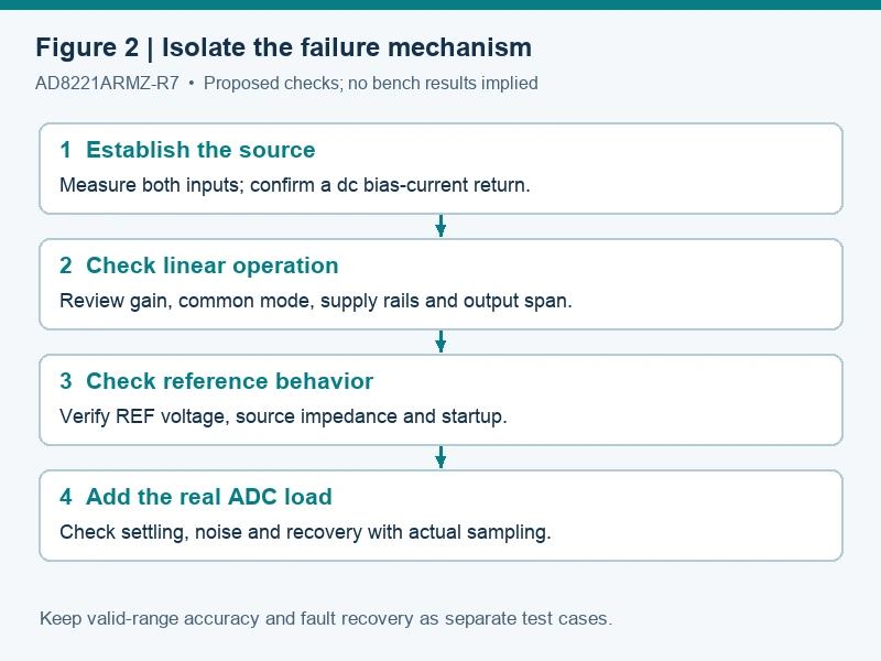
Start debugging with a slow, controlled differential input and a known common-mode voltage. Record both input pins, REF, the supply rails, and the output. Repeat near the intended endpoints before adding fast sampling activity. If the static transfer is correct but the sampled reading changes when the ADC runs, the acquisition path deserves attention. If the static output is already pinned, inspect the input region, reference, and gain before changing digital filtering.
Fault recovery should be tested separately from valid-range accuracy. An open bridge lead, excessive input voltage, or a supply starting late can produce conditions absent from a normal transfer sweep. The datasheet's input protection discussion has specific current and voltage conditions; it is not a complete industrial surge qualification. Select external protection against the actual installation requirements, then verify its leakage, capacitance, and imbalance during normal measurement.
For static load measurement, also avoid adopting an AC-coupled application without checking its purpose. An integrator that removes dc can be useful for an AC signal riding on offset, but the dc component is often the quantity a weighing system needs to retain. Application circuits should be transferred according to their signal assumptions, not just because the same amplifier appears in the drawing.
An alternative earns a place on the shortlist when it changes a relevant tradeoff, such as source loading, supply range, bandwidth, or output headroom. The following four Analog Devices ordering models are identified on their official product pages. They are comparison candidates for instrumentation-amplifier signal conditioning. None has been qualified here as a direct replacement for AD8221ARMZ-R7.
Table 5. Four related candidates and the checks their differences create.
| Exact candidate | Shared role | Family-level distinction supported by the official page | Compatibility work still required |
|---|---|---|---|
| AD8220ARMZ-R7 | Instrumentation amplifier, eight-lead MSOP option | JFET inputs and rail-to-rail output | Input-current limits for the chosen grade, headroom, gain equation, pinout, and stability |
| AD8226ARMZ-R7 | Instrumentation amplifier, eight-lead MSOP option | Wide supply range, including 2.2 V single-supply operation, and rail-to-rail output | Offset, noise, gain resistor, source range, temperature, and ADC interface |
| AD8421ARMZ-R7 | Instrumentation amplifier, eight-lead MSOP option | Low-noise, high-speed family intended for faster precision signal paths | Bandwidth and settling needs, supply current, layout, gain resistor, and exact-grade limits |
| AD8422ARMZ-R7 | Instrumentation amplifier, eight-lead MSOP option | Low-power family with rail-to-rail output | Loaded output swing, reference behavior, offset drift, gain equation, and package connections |
Sources: official AD8220, AD8226, AD8421, and AD8422 product pages, including model/package listings. Family descriptions identify comparison directions; they do not transfer another grade's headline specifications to these ordering codes.
For a high-impedance source, the JFET-input candidate gives a concrete reason to revisit the current-related error budget. For a lower supply rail, the wider-supply candidate gives a different starting point for headroom. A faster acquisition task may justify examining the high-speed family, while a design losing too much output span near the rails may benefit from evaluating a rail-to-rail-output architecture. Those are reasons to investigate, not conclusions that one candidate is better in every bridge system.
Run the same worksheet for each candidate. Keep sensor excitation, source impedance, bandwidth, temperature range, load, and calibration method fixed while comparing the amplifier. Otherwise one part may appear quieter simply because it was assessed over less bandwidth, or more accurate because its typical value was compared with another part's guaranteed maximum. Comparable conditions are more valuable than a long list of isolated specifications.
Do not preserve the existing gain resistor automatically when changing families. Likewise, an eight-lead MSOP description does not by itself establish a safe PCB substitution. Check the exact pin assignment, footprint, reference connection, operating limits, and power-up behavior. If those checks reveal a board change, describe the candidate as a redesign option and budget its verification effort accordingly.
The selection decision should leave behind a short set of reproducible tests. First verify the static transfer across the intended differential and common-mode range. Next check the required temperature and supply corners. Then run the actual ADC sampling pattern and evaluate noise over the intended display or control bandwidth. Finally exercise relevant faults and confirm recovery. Each stage answers a different question, so a successful room-temperature sweep should not stand in for the rest.
Include a common-mode rejection check in that plan. Hold the differential input constant while varying the common-mode voltage over the range the installation can produce. Observe whether the output moves by more than the allocated error. Keep both input paths representative of the real source, because an artificially balanced bench fixture can hide cable or filter mismatch. This test addresses interference conversion and operating-region behavior; it should be distinguished from a differential gain sweep.
For calibration, take zero and span readings only after defining a repeatable stabilization condition. Apply intermediate loads or electrical input steps to check whether a two-point correction leaves acceptable residual error across the useful range. Then repeat selected points after a temperature change or a relevant power cycle. Save the uncorrected readings and the correction coefficients together. If calibration appears to fix one endpoint while an intermediate point remains wrong, investigate nonlinearity, saturation, sensor mechanics, or settling before adding more correction terms. A more complicated formula can conceal an analog problem without making the measurement trustworthy.
Record the sensor or source emulator, excitation, gain resistor, reference source, load, sampling rate, filtering, and temperature with each result. A graph without those conditions is difficult to compare with a later board revision. Save raw readings as well as any averaged display values so that a quiet presentation does not conceal occasional saturation or settling errors.
AD8221ARMZ-R7 is a reasonable candidate when its precision instrumentation-amplifier behavior fits the bridge's signal level and the available headroom. Its selection case is strongest when the ARM-grade error budget closes, the common-mode and output requirements coexist, and the converter interface has been verified. If one of those conditions fails, the four related candidates provide specific directions for further evaluation. Confirm the complete ordering code and required packaging when sourcing, and keep the engineering qualification attached to that exact choice.