
Scarlett Zhang



21 views

| Picture | Part Number | Manufacturer | Stock | Action |
|---|---|---|---|---|
 | 1ED020I12-F2 | Infineon | 5,770 | |
 | 1ED020I12-B2 | Infineon | 2,990 |
No. Infineon separately lists the F2's isolation type as functional. Match the exact documented insulation properties to the system requirement rather than inferring the category from voltage class.
This article does not establish that. It is a related device with a different isolation classification. Any proposed replacement requires its own electrical, timing, package, qualification, and system review.
Not on the basis of nominal voltage alone. The F2 logic table requires at least 3.5 V for a guaranteed high input. Check the complete interface, including returned status signals, and provide a suitable voltage-domain interface when needed.
No. The datasheet explicitly states that VEE2 is not monitored by the output UVLO function. A design depending on negative gate bias must address that rail separately.
1ED020I12-F2 is Infineon’s single-channel isolated gate driver with DESAT protection and an active Miller clamp. Infineon classifies its isolation as functional, which is a decisive selection boundary when comparing it with similarly named drivers. This guide separates isolation classification from voltage class, then reviews the logic interface, gate supply, fault timing, and layout conditions that determine whether the device fits a particular power-stage design.
Infineon's product page identifies 1ED020I12-F2 as a functional-isolation device. The nearby 1ED020I12-B2 is classified as basic isolation and has separate certification information. The similar names, output-current figures, and package style do not make the isolation claims interchangeable. Infineon F2 product page, Infineon B2 product page.
The selection question is whether the exact device's documented insulation category and ratings satisfy the role assigned to that barrier in the complete equipment. A functional-isolation listing does not establish basic or reinforced safety insulation. Conversely, selecting a component with a different isolation category does not by itself establish compliance for the entire board or product. The equipment's insulation requirements, operating conditions, spacing, and other barrier components must be considered together.
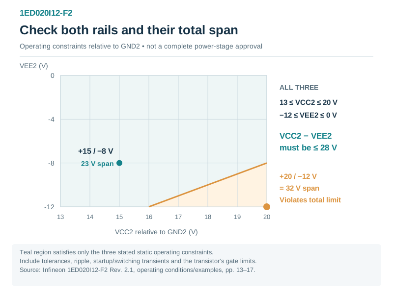
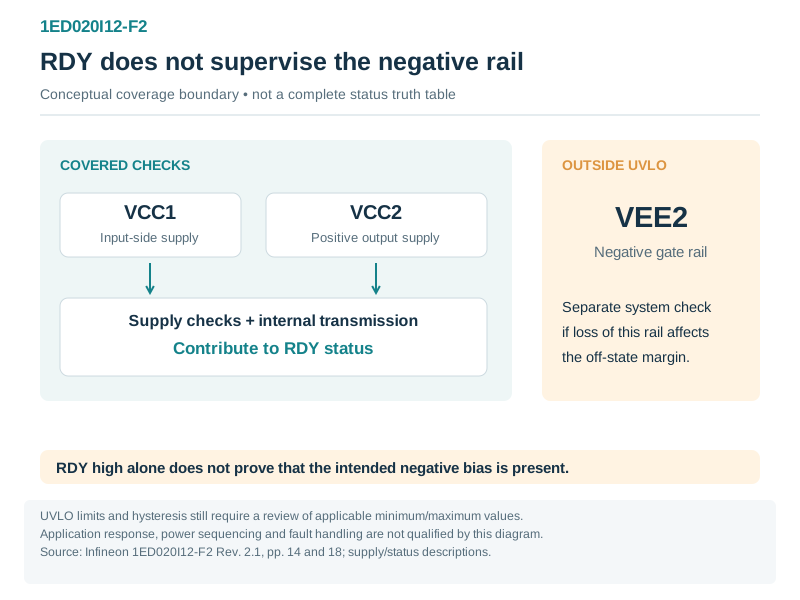
**Figure 1. 1ED020I12-F2 gate supplies must satisfy individual and span limits.** Operating-range screen for 1ED020I12-F2 with both rails referenced to GND2: 13 V ≤ VCC2 ≤ 20 V, −12 V ≤ VEE2 ≤ 0 V, and VCC2 − VEE2 ≤ 28 V. The +15/−8 V example gives 23 V span; +20/−12 V gives 32 V and violates the joint limit. The shaded region checks only these static driver-supply constraints; tolerances, transients, transistor gate limits and isolation requirements still need review. Sources: [supporting source 1](https://www.infineon.com/assets/row/public/documents/24/49/infineon-1ed020i12-f2-datasheet-en.pdf). **Figure 2. 1ED020I12-F2 readiness does not monitor the negative gate rail.** Conceptual supervision boundary for 1ED020I12-F2. UVLO monitors the input-side and positive output-side supplies, while RDY also reflects internal-transmission conditions. VEE2 is outside this UVLO coverage; a high RDY does not prove that the intended negative gate voltage is present. The application must define its own response if loss of VEE2 affects off-state margin. This is not a complete truth table, protection design or safety qualification. Sources: [supporting source 1](https://www.infineon.com/assets/row/public/documents/24/49/infineon-1ed020i12-f2-datasheet-en.pdf).Keep four items distinct in the selection record: the power switch's voltage rating, the driver's voltage class, the driver's isolation classification, and the complete system's insulation requirement. Treating them as one “1200 V” field hides the decision that matters most.
A gate driver may correctly transfer a switching command across galvanically separated domains while still being unsuitable for the safety role intended for that barrier. Establish that role before spending time optimizing gate resistance or comparing peak drive current.
The final datasheet is explicitly for 1ED020I12-F2, Rev. 2.1 dated September 27, 2017. It identifies the PG-DSO-16-15 package. Infineon's product page separately maps the product to orderable code 1ED020I12F2XUMA1. The manufacturer's product name should remain visible in the engineering discussion, while a purchasing release should record the full confirmed orderable code and actual packing. This mapping does not establish the packaging of an unidentified physical lot. Infineon product ordering information.
Table 1. Identity and isolation comparison. Source: the respective F2 and B2 manufacturer pages, checked September 20, 2026. Compiled by YG Group; this is not a substitution approval.
| Item | 1ED020I12-F2 | 1ED020I12-B2 |
|---|---|---|
| Role in this guide | Primary device | Related comparison |
| Manufacturer isolation classification | Functional | Basic |
| What can be concluded | Use the F2's own insulation and electrical evidence | Review the B2's own evidence for a proposed change |
| What cannot be transferred | Another device's certification or insulation category | Automatic approval for an existing F2 board |
The comparison is intentionally narrow. It answers why the suffix matters without implying that the B2 is a universal upgrade or that its other electrical details have been qualified for a particular circuit.
The F2 input side is designed around a nominal 5 V supply. Its operating VCC1 range is 4.5–5.5 V, and the logic table specifies a high-input threshold of 3.5 V minimum for IN+, IN−, and reset. A nominal 3.3 V microcontroller output therefore cannot be assumed to provide a guaranteed valid high level. Check the controller's guaranteed output voltage at the actual load and operating conditions; use a suitable interface if the margin is insufficient. F2 Rev. 2.1, pp.17 and 19.
This is an easy issue to miss because the device is described as microcontroller-compatible. That description applies within the stated 5 V CMOS conditions. It is not a claim that every contemporary MCU voltage is directly compatible.
The command inputs also have defined polarity. In normal operation, the on condition requires IN+ high and IN− low. Reset low disables the input logic. Document these states in the schematic and firmware interface, including what happens while the controller is starting, resetting, or unpowered.
RDY and /FLT are status outputs with open-drain behavior and the specified internal pull-up characteristics. Review their voltage domains, pull-up network, and receiving input limits. In particular, do not make a 3.3 V controller connection safe merely by addressing the command direction while overlooking the returned status signals.
The input pulse-suppression specifications are also part of the timing contract. Narrow pulses are filtered, so a controller's shortest generated pulse must be assessed against the driver behavior. A pulse that appears in a logic capture at the MCU pin is not automatically a valid gate command at the output.
The driver supports both unipolar and bipolar output-side supplies. The datasheet illustrates +15 V/−8 V operation and a unipolar +15 V arrangement. These examples show different ways to manage the off-state gate, not two universally suitable supply choices for every power transistor.
The operating table gives VCC2 as 13–20 V relative to GND2, VEE2 as −12–0 V relative to GND2, and a maximum difference VCC2 − VEE2 of 28 V. The individual limits and the total span must all be satisfied. Selecting +20 V and −12 V because each appears in a separate row would produce 32 V between the rails and violate the span limit. F2 Rev. 2.1, pp.13–17.
Include supply tolerance, ripple, startup overshoot, and switching transients in that comparison. Nominal voltages are insufficient when the design operates close to a boundary. The power transistor's permitted gate voltage imposes another limit that may be tighter than the driver supply range.
The nominal ±2 A drive-current description concerns peak gate-driving capability under the relevant conditions. It is not a continuous output-current rating and does not directly determine switching time for an arbitrary IGBT. The gate-charge profile, gate resistance, driver output behavior, and layout inductance determine the resulting waveform.
A useful design process starts with the actual power transistor and the desired switching behavior, then checks whether the driver can supply and remove the required gate charge within acceptable losses and voltage excursions. It does not start by dividing a single capacitance value by the headline current and treating the answer as a guaranteed switching time.
The F2 monitors the input-side and positive output-side supplies with undervoltage lockout. The datasheet gives typical input thresholds around 4.1 V on and 3.8 V off, and output thresholds around 12 V on and 11 V off, with separate limit and hysteresis specifications. A design should use the applicable limits and behavior rather than only the typical values. F2 Rev. 2.1, pp.14 and 18.
A particularly important boundary is that VEE2 is not monitored by this UVLO function. In a bipolar gate-supply design, RDY high therefore does not prove that the negative gate rail is present at its intended voltage. If that rail is important to the off-state margin, its failure needs a separate system-level response.
RDY reflects the monitored supply and internal-transmission conditions. /FLT reports a desaturation event. Keep those meanings separate in the controller's state machine. Combining them into an undifferentiated “driver good” flag can lose useful fault information and encourage incorrect restart behavior.
The active shutdown function helps hold the gate off under its specified unpowered-output conditions. Its table gives a defined test condition; it is not a blanket guarantee for every disconnected rail, external injection current, or damaged interconnect. Review power-up and power-down as actual circuit states, including the gate's discharge path and the controller's behavior.
DESAT monitors a voltage related to the power transistor's on-state collector-emitter voltage through the external network. It is not a direct current measurement. The diode, series components, blanking capacitor, parasitic capacitance, and switching behavior all affect the signal that reaches the DESAT pin.
The F2's desaturation reference is 9 V typical, with an 8.3–9.5 V range in the cited table. Its capacitor-charge current is 500 µA typical, with 450–550 µA limits under the stated conditions. The external capacitor therefore participates in a timing decision, rather than serving simply as a noise filter that can be enlarged without consequence. F2 Rev. 2.1, pp.15 and 22.
For a first-order calculation, charging a capacitor through a constant current takes approximately t = C × ΔV / I. This estimates one part of the blanking behavior. It does not include every internal delay, the actual starting voltage, external diode behavior, or the gate-discharge interval. Use the full timing diagram and the relevant limits to construct the protection budget.
The distinction between gate turn-off and fault reporting is crucial. Table 11 lists DESAT-sense-to-output timing separately from DESAT-sense-to-/FLT timing. The latter can take up to 2.25 µs under its specified test conditions. The logic-status transition is therefore not an instantaneous timestamp for the start of gate turn-off.
Table 2. Elements of the DESAT review. Source: Infineon F2 Rev. 2.1, pp.15, 19, 22 and 25. Design implications compiled by YG Group.
| Element | What it controls | Required review |
|---|---|---|
| External sensing path | Relationship between transistor voltage and DESAT voltage | Diode behavior, voltage stress, parasitics, and routing |
| Blanking capacitor and charge current | Delay before the threshold can be reached | Component tolerance, current limits, startup level, and switching transient |
| Internal filtering and output delay | Response after the detection condition | Applicable timing definitions and load conditions |
| Gate discharge | Time until the transistor actually turns off | Gate resistor, charge profile, driver behavior, and waveform |
| /FLT reporting | Controller notification | Status latency and controller capture behavior |
| /RST command | Fault reset and enable behavior | Minimum reset duration and controlled restart policy |
The acceptable total time depends on the power transistor's short-circuit capability under the actual voltage, gate bias, and temperature conditions. This guide does not approve a protection circuit for a specific IGBT. Its purpose is to identify the timing terms that must be compared.
The datasheet also describes a case in which an off command during the DESAT-to-fault delay erases the fault status. Firmware and fault logging should account for that behavior. A later high /FLT level is not sufficient evidence that no transient event occurred.
During switching in a half bridge, changing voltage across the off-state transistor can couple current through its Miller capacitance and raise its gate voltage. The active Miller clamp provides a local sinking path after the gate has fallen to the clamp activation region.
For this device, Table 8 specifies a clamp threshold relative to VEE2: 2.1 V typical, with 1.6–2.4 V limits. The pin-description prose contains an inconsistent “below” phrasing, so the numerical table and functional description are the appropriate references for interpreting the threshold. It should not be read as requiring the gate to fall 2 V below the negative rail. F2 Rev. 2.1, pp.11, 15 and 20.
The clamp's physical path matters. A long route between the gate and CLAMP pin adds impedance to the path intended to suppress an unwanted gate rise. Inspect the loop with the transistor emitter/reference connection, not just the net name in the schematic.
Short-circuit clamping is a different feature. It addresses a gate-voltage rise during a short-circuit condition through paths associated with OUT and CLAMP. Its current and duration limits must be respected; it should not be treated as unlimited gate overvoltage protection.
A negative gate supply and an active clamp are design tools with different dependencies. Neither should be removed solely because another circuit used only one. Validate the off-state gate waveform for the actual transistor, layout, bus conditions, and switching speed.
The datasheet's PCB guidance calls for spacing between the low-voltage and isolated high-voltage circuitry, short bypass routes, and attention to adjacent isolated high-side sections. The package alone does not define the complete board barrier: copper pours, vias, test points, and nearby components can determine the shortest path.
Thermal performance is layout-dependent as well. The F2 uses the GND1 and VEE2 pin connections as important heat paths, and the reference thermal layout specifies a particular copper arrangement. Do not combine the published thermal resistance with an unrelated minimal-copper board and assume the same temperature rise. F2 Rev. 2.1, pp.16–17 and 27.
Increasing copper for heat spreading must preserve the intended isolation spacing. Keep the low-side and isolated-side thermal copper within their respective domains. Review the completed layout after all thermal changes, because a well-intended copper addition can change the barrier geometry.
A selection review should finish with a validation plan covering logic levels, supply sequencing, gate waveforms, fault response, and temperature. Use measurement equipment and probing appropriate to the voltage domains; the resulting records should identify the exact setup and conditions. No test results are asserted here.
Select 1ED020I12-F2 by first establishing the required isolation role, then verifying the exact logic, supply, and protection conditions. Functional isolation, peak gate current, DESAT response, and Miller clamping each answer a different design question. Keeping those questions separate produces a clearer component choice and a more useful validation plan for the complete power stage.
By Scarlett Zhang