
Alice Chen



3 views

| Picture | Part Number | Manufacturer | Stock | Action |
|---|---|---|---|---|
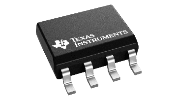 | THVD1420DR | Texas Instruments | 2,210 | |
 | THVD1420DRLR | Texas Instruments | 3,890 | |
| THVD1400DR | Texas Instruments | 9,580 | |
| THVD1400DRG4 | Texas Instruments | 2,910 | |
| THVD1400DRLR | Texas Instruments | 4,250 |
No. It identifies the standard large-reel packing for THVD1420DR. Commercial order quantities and alternative carrier formats depend on the actual offer. Confirm the delivered packing rather than assuming a smaller order will arrive on a full factory reel.
The transceiver's input thresholds permit useful compatibility in that direction, but the complete interface requires another check: its receiver output R is referenced to the 5 V transceiver supply. Verify the MCU receive pin's voltage tolerance and powered-off limits before approving the connection.
The illustrated surge application uses THVD1400. It should not be represented as a THVD1420DR 12 Mbps test. A fast-link design must qualify its own protection, cable, layout, and operating conditions.
By Alice Chen
THVD1420DR is a Texas Instruments half-duplex RS-485 transceiver with a 12 Mbps maximum signaling rate, a 3.0–5.5 V operating supply, and an eight-pin SOIC package. A production-ready BOM must also define its cable interface, protection network, logic compatibility, assembly packaging, and approved substitutions. This guide turns those dependencies into a release checklist so purchasing and manufacturing receive a buildable interface specification, rather than an isolated transceiver part number.
For a schematic, “THVD1420” identifies the electrical family. For a purchase order, it leaves important choices open. THVD1420DR is the eight-pin SOIC version supplied in large tape and reel. The small SOT package also illustrated in the family datasheet has a different footprint. It is not what the DR suffix orders.
TI's exact-part page identifies THVD1420DR as an active catalog device, with a −40°C to +125°C operating temperature range and a standard package quantity of 2,500. That status was checked on September 20, 2026; it is not a delivery commitment. Reel quantity is a packaging attribute, not automatically the supplier's minimum order quantity. A quotation must state whether delivery is a factory reel, custom reel, or cut tape. TI exact-part information.
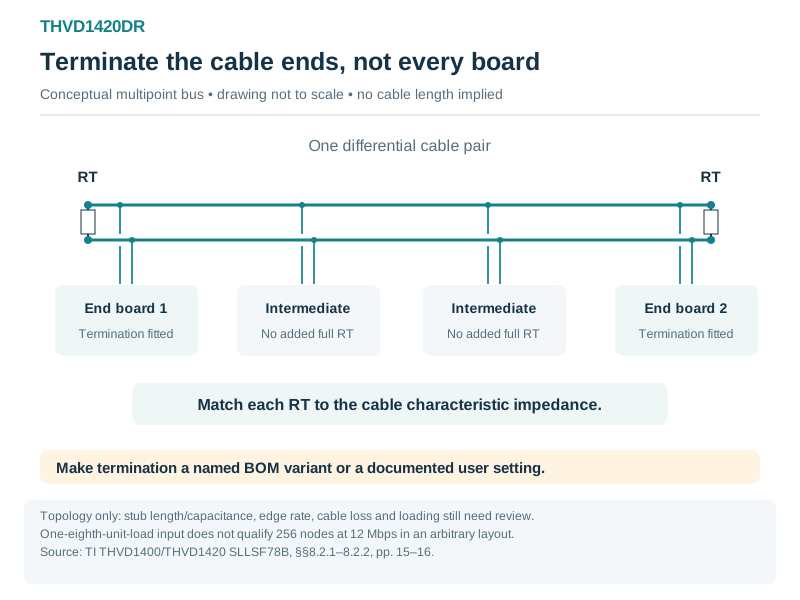
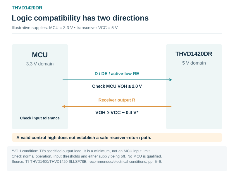
**Figure 1. THVD1420DR bus termination follows installation position.** Conceptual multipoint RS-485 topology: fit cable-matched termination at the two cable ends and normally omit additional full terminations at intermediate nodes. This is an installation-role and BOM-control diagram, not a complete schematic or a validated cable layout. Stub geometry, capacitance, edge rate, loss and loading still need review; no 12 Mbps distance or 256-node configuration is qualified. Sources: [supporting source 1](https://www.ti.com/lit/gpn/THVD1420). **Figure 2. THVD1420DR logic compatibility must close in both directions.** Illustrative voltage-domain review with a 3.3 V MCU and THVD1420DR at VCC = 5 V. The MCU’s guaranteed output must meet the transceiver’s 2.0 V high-input requirement; receiver output R has VOH ≥ VCC − 0.4 V under the specified load condition. These are different checks. Verify MCU input tolerance, thresholds and powered-off behavior; no unspecified MCU or direct connection is qualified here. Sources: [supporting source 1](https://www.ti.com/lit/gpn/THVD1420).Not on the evidence of the shared family alone. Its 500 kbps maximum rules it out for faster links, and compatible slower applications still need a timing and circuit review before AVL approval.
Table 1. Identity fields to freeze before requesting volume quotations
| BOM field | THVD1420DR entry or release requirement | Why it matters |
|---|---|---|
| Manufacturer and full MPN | Texas Instruments; THVD1420DR | Prevents a family-name quote from concealing package differences |
| Package | SOIC, eight pins, TI package code D | Distinguishes the installed footprint from the SOT/DRL alternative |
| Nominal body | 4.90 × 3.91 mm | Supports package identification; the mechanical drawing controls tolerances |
| Assembly carrier | Standard large tape and reel; 2,500 devices per reel | Lets the assembler plan feeders and purchasing compare the offered packing |
| Finish and handling | NiPdAu; listed MSL 1, 260°C peak classification | Check the actual shipment label and the assembler's qualified process |
| Design document | SLLSF78B, revised October 2021, plus the current packaging addendum | Keeps schematic review tied to an identifiable revision |
| Approved substitute | None unless individually qualified in the project's AVL | A related part number is not an automatic production authorization |
Source: TI datasheet, device information, package option addendum, and SOIC D0008A drawing; exact-part page checked September 20, 2026. Compiled by YG Group.
Keep the engineering revision of the circuit separate from the manufacturer's document revision. If a protection resistor or termination option changes, the assembly BOM must show that change even when the transceiver MPN stays the same. Conversely, an updated manufacturer datasheet should trigger a review of the affected requirements, not an unexplained change to the released circuit.
The transceiver has one differential pair, A and B, shared between transmit and receive. It does not provide galvanic isolation, a communications protocol, or a guaranteed cable length at the maximum data rate. Those are system decisions.
Begin the design record with the actual bus: point-to-point or multipoint, intended signaling rate, cable characteristic impedance, longest cable, stub arrangement, connectors, ground reference, and the electrical environment at each port. Then identify which boards sit at the two cable ends. This determines where termination is fitted and avoids giving every node an unconditional termination resistor.
The datasheet recommends termination at the two ends of the bus, with resistor values matched to cable impedance. Intermediate nodes normally should not create additional full terminations. Its one-eighth-unit-load input specification describes receiver loading; the advertised node count does not establish that a particular 256-node cable layout will work at 12 Mbps. Stub capacitance, edge reflections, cable loss, and termination all remain relevant. TI datasheet, Sections 8.2.1–8.2.2, pp. 15–16.
For a product offered in several installation roles, make the termination a controlled assembly option or a clearly documented user setting. An unlabelled resistor marked “DNP if not required” transfers a circuit decision to manufacturing. The release package should name the board variant, fitted state, and installation role.
Bus polarity also belongs in the drawing. In TI's truth table, a high driver input produces A high and B low, with differential voltage defined as VA minus VB. Map that behavior to the connector's actual pin labels and the remote equipment's convention. Copying “A” and “B” names between unrelated equipment is insufficient evidence that the physical wiring is correct. TI datasheet, Section 7.4, p. 13.
The THVD1420 recommended supply range is 3.0–5.5 V. Its driver-input and enable-input high threshold is 2 V minimum, while the permitted high input range extends to 5.5 V. This helps a 3.3 V MCU control a transceiver powered from 5 V. It does not, by itself, establish that the return path from the receiver output to that MCU is safe.
The receiver output R follows the transceiver's supply domain. TI specifies a high output of at least VCC minus 0.4 V under its stated load condition. With a 5 V transceiver supply, the MCU receive input therefore needs suitable voltage tolerance or a properly designed interface. Check the MCU's allowed input voltage, powered-off behavior, and input thresholds. A schematic note that says “3.3 V logic compatible” can hide this direction-dependent problem. TI datasheet, recommended operating conditions and electrical characteristics, pp. 5–6.
Table 2. Electrical boundaries that should appear in the design review
| Check | Datasheet boundary | Production implication |
|---|---|---|
| Supply | VCC = 3.0–5.5 V, recommended | Include tolerance, ripple, startup, and connector transients |
| Logic controls | D, DE, and active-low RE have specified input thresholds | Verify actual MCU output levels and reset behavior |
| Receiver output | R is referenced to the transceiver supply | Verify the MCU input in normal operation and with either rail off |
| Bus operating voltage | Each bus terminal is specified from −7 V to +12 V under recommended conditions | Include ground offset in the cable-interface assessment |
| Bus stress limit | ±16 V is an absolute maximum rating | Do not describe sustained operation throughout this range |
| Temperature | Ambient range −40°C to +125°C, subject to junction-temperature limits | Include self-heating and the board's thermal environment |
Source: TI datasheet, pp. 4–6. Compiled by YG Group. Absolute maximum ratings are stress limits; they are not extended operating specifications.
If the ground-offset requirement exceeds the available operating margin, changing the TVS alone does not solve the architecture. The design may require isolation and an appropriate isolated supply, together with a fresh system-level protection review. Those additions change the BOM, board space, and qualification plan substantially. Decide this before treating the interface as a routine eight-pin component purchase.
DE is active high; RE is active low. The device includes weak internal biasing that disables the driver and receiver when the respective enable inputs are left open. A production design should nevertheless document the MCU reset state and the intended bus behavior during boot, firmware update, watchdog reset, and power loss. External pull resistors may be appropriate when a deterministic state must hold against board leakage, noise, or another connected circuit. Their values should be chosen for that circuit, not copied without checking.
A particularly important timing distinction is whether the device is waking from shutdown. With the receiver already enabled, the driver's enable timing is specified on a nanosecond scale. When the receiver is disabled and the device must wake, the driver-enable maximum is 10 microseconds under the specified test conditions. Receiver wake-up also depends on the driver's state. At 12 Mbps, one bit is about 83 ns, so enabling the device and immediately transmitting can lose the start of a frame. TI datasheet, switching characteristics and measurement circuits, pp. 7–8 and 11–12.
The firmware release requirements should distinguish three events: waking the transceiver, enabling the transmitter, and releasing the bus after the final bit. Use the relevant maximum timing for each event, add the controller's actual timing uncertainty, and validate with an oscilloscope at the intended operating conditions. A UART transmit-complete event may be useful, but its precise meaning must be checked in the controller documentation; a buffer-empty event is not necessarily the end of the last stop bit.
These are manufacturing concerns as well as firmware concerns. A board may pass a slow bench demonstration and still fail an automated test that starts a transaction immediately after applying power. Define the startup wait and the test fixture's bus state in the production test specification.
TI specifies bus-pin IEC contact ESD, air-discharge ESD, and fast-transient performance. These are useful component-level capabilities. They do not certify the completed enclosure, connector, PCB, and power system against every disturbance. Surge energy, discharge location, return paths, and the applicable equipment test setup still determine the protection network.
The family datasheet contains a useful example with series pulse-proof resistors and a TVS. However, its illustrated 1 kV surge application is a THVD1400 circuit. The example uses a slower, 500 kbps member of the family; the accompanying waveform is not a THVD1420 12 Mbps validation. Treat the listed Bourns CDSOT23-SM712 and Vishay CRCW0603010RJNEAHP parts as components in that stated example, not as a universally approved THVD1420DR protection BOM. TI datasheet, surge protection example and component table, pp. 18–19.
For a THVD1420DR design, qualify candidate protection parts against both the disturbance and the signal:
These checks may lead to an approved set of protection alternatives, but each alternative needs the relevant electrical and layout evidence. A purchasing substitution based only on “same voltage, same package” can change clamping or capacitance enough to invalidate prior tests.
A useful interface BOM is a short set of controlled functions. It need not overpopulate the PCB; it must explain why each fitted or optional position exists.
Table 3. Recommended release fields for the interface BOM
| Function | What to specify | Evidence or validation to retain |
|---|---|---|
| Transceiver | THVD1420DR, TI, package and carrier requirements | Exact-part identification; approved PCB footprint |
| Local bypass | Ceramic capacitor at VCC and GND; value and voltage rating | TI recommends 100 nF close to the pins; confirm the selected part's effective capacitance and layout |
| End termination | Resistance matched to the selected cable; tolerance, power, fitted variant | Cable specification and tested topology |
| External bias, if used | Resistor values, rail, and fitted state | Bus loading and idle differential-voltage calculation, including all nodes |
| TVS and series protection, if required | Exact approved MPNs and pulse/capacitance requirements | System protection test and signal-integrity test on the released layout |
| Connector and cable | Pinout, polarity, reference/shield treatment, approved mating parts | Harness drawing and interoperability test |
| Enable-state resistors, if used | Required default state and value | Reset, startup, and powered-off tests |
| Assembly options | Explicit DNP/fitted rules linked to each board variant | Manufacturing work instructions and inspection criteria |
Source: design-release framework compiled by YG Group from TI datasheet, application, supply, and layout guidance, pp. 15–21. Project-specific choices require project validation; this is not a tested reference design.
The on-chip failsafe behavior makes the receiver output high for specified open, shorted, and idle conditions. It does not tell application software which condition occurred. A product that must detect a broken cable still needs protocol-level diagnostics or a separate diagnostic strategy. Likewise, a failsafe receiver does not automatically justify removing external bias from a bus containing other receiver types. Evaluate the whole network. TI datasheet, receiver function table, p. 14.
THVD1400DR is a useful related part because it shares the SOIC package option and the family interface arrangement. Its maximum signaling rate is 500 kbps, compared with 12 Mbps for THVD1420DR. It cannot replace the faster part in a design that needs more than 500 kbps.
Even below that limit, qualification should cover timing, edges, the protection network, and the intended cable topology. Slower edges can alter reflections and emissions, but this does not establish that every THVD1400 implementation is interchangeable with a THVD1420 implementation. The respective switching-characteristic tables must govern the review. TI datasheet, pp. 7–8.
Keep THVD1400DR as an engineering alternative under evaluation until the project has approved its configuration. If it is eventually accepted, record any restrictions in the AVL: maximum firmware baud rate, compatible product variants, and required test coverage. A procurement system should not silently substitute it solely because the family names differ by two digits.
Request quotations against the full MPN and an agreed delivery configuration. Include quantity, required delivery schedule, packaging condition, traceability documentation, and any approved lot or date-code constraints. Confirm the offered manufacturer identity and part marking against the manufacturer's information, while recognizing that marking alone is not a complete authenticity assessment. Avoid turning an unverified “equivalent” into a production line item.
For the assembly handoff, attach the SOIC D0008A package and land-pattern reference. The datasheet also contains DRL drawings, so the assembler should not select the first eight-pin drawing it encounters. Check feeder orientation and pin 1, solder-mask and paste choices, the actual shipment label, and the assembly site's qualified reflow profile. TI's example land and stencil drawings are starting points, not proof that every PCB process has identical tolerances.
A practical release test should answer four questions. First, does the device communicate correctly at the required supply and temperature limits on the intended cable? Second, does startup and transmitter turnaround remain reliable through the actual firmware sequence? Third, do the chosen protection parts preserve the signal while meeting the project's disturbance tests? Fourth, can manufacturing reproduce those results using the released board variant, assembly process, and test fixture?
Keep the answers attached to a configuration: PCB revision, firmware revision, transceiver MPN, protection MPNs, cable, termination state, and test conditions. Without that record, a passing result is difficult to reuse after an engineering change. Do not label a calculated margin or a planned test as a measured result.
A THVD1420DR volume BOM is ready when it identifies the exact orderable device and the circuit conditions that make it usable. Freeze the termination options, close the MCU voltage check in both directions, specify wake-up timing, and qualify the protection network at the real data rate. Give purchasing and manufacturing the resulting configuration and evidence, including the limits on any alternative. That is what allows repeat builds to reproduce an approved RS-485 interface.