
Carmen Lau




| Picture | Part Number | Manufacturer | Stock | Action |
|---|---|---|---|---|
 | TPS51200DRCR | Texas Instruments | 2,190 | |
 | TPS51206DSQR | Texas Instruments | 7,100 | |
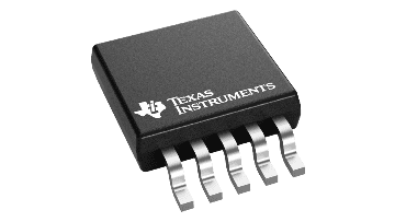 | TPS51100DGQR | Texas Instruments | 7,910 | |
 | TPS51216RUKR | Texas Instruments | 3,530 | |
 | LP2998MRX/NOPB | Texas Instruments | 3,740 |
Its main task is the bidirectional termination rail and reference buffer. The memory VDDQ rail normally comes from another supply. Define the exact FPGA and DRAM architecture before assuming an external VTT rail is required.
Terminated signals can demand current from VTT or return current to it. Calculate both directions from the termination network and switching conditions. A regulator designed only to source current cannot automatically perform this role.
No. The supplied electrical table specifies the relevant REFOUT accuracy with a narrower ±1 mA test range. Drive capability and precision under a stated load are separate specifications. Include all reference loads in the budget.
Do not decide from the printed value alone. Follow the detailed application guidance, including effective capacitance, ESR, local placement and sense routing. DC bias and tolerance can reduce the capacitance available on the powered board.
Category: Applications&Solutions
Author: Carmen Lau
TPS51200DRCR can supply a tracking, bidirectional DDR termination rail on an FPGA network board when the memory topology requires external VTT. Its useful features are source-and-sink regulation, a separate buffered reference and remote sensing. The design still depends on the exact memory interface: current demand, effective output capacitance, reference loading, sequencing and board heat flow must be verified. A “3 A termination regulator” headline alone does not establish an acceptable DDR rail.
An FPGA network board may use external memory for packet buffers, tables or processing state. That application context explains why reliable memory power matters, but it does not identify a particular FPGA, memory generation or termination topology. This article uses a hypothetical board and TI's published DDR examples. It does not claim that TPS51200DRCR has been qualified in an unnamed customer design.
Begin with the FPGA memory-controller guidance and the selected DRAM documentation. Identify which signals use external termination, which use on-die termination, what reference voltages are required and how the rails must behave during startup and shutdown. A regulator advertised for several DDR generations does not make those interfaces electrically identical. The board's termination network defines the load presented to VTT.
The key difference from a conventional supply is current direction. When a terminated signal is driven high, current may flow into the VTT rail; when driven low, the termination rail supplies current toward ground. The regulator must hold the intended voltage in both cases and through transitions. An ordinary source-only regulator can behave poorly when the termination network returns current into its output.
No. PGOOD detects a much broader output departure than the interface may tolerate. Validate VTT tracking, transients and the memory interface itself across the intended voltage, temperature and operating conditions.
They can cancel as signed average current while both operating states dissipate power. Calculate sourcing and sinking losses separately and average their power over time. Verify heat removal through the exposed pad and actual PCB.
TPS51200 addresses this task with a tracking linear regulator. VO supplies the termination power, VOSNS observes the selected regulation point, and REFOUT provides the buffered reference against which VO is controlled. Keeping those roles distinct prevents a common schematic error: treating the low-current reference output as another place to connect the power termination network.
The exact TPS51200DRCR is a 10-pin DRC VSON device with a nominal 3 × 3 mm body, supplied in the large tape-and-reel option. The supplied addendum lists 3,000 units and a −40 to +85°C operating temperature range. TI's current exact-code page confirms the orderable identity. The catalog device should not inherit automotive qualification from TPS51200-Q1, which is a separately identified version. TI exact part record.
The bias input VIN operates from 2.375 to 3.5 V. It is usually connected to a suitable 2.5 V or 3.3 V rail. VLDOIN is the power input for the linear stage; the application guidance gives 1.1–3.5 V for that input. REFIN accepts the reference, with a specified operating range of 0.5–1.8 V. In a typical DDR arrangement, an equal resistor divider derives REFIN from VDDQ.
These ranges should not be confused with absolute maximum ratings. In particular, a nominal 5 V supply cannot be connected directly to VIN merely because other board circuits use it. If the available bias architecture is 5 V, a different regulator or a suitable preceding supply is required. Also check the lowest instantaneous VIN during board activity: a nominal 2.5 V rail has limited room above the 2.375 V minimum.
Table 1: The three voltage roles in a TPS51200DRCR design
| Node | Role and published guidance | Design check |
|---|---|---|
| VIN | Bias supply, 2.375–3.5 V | Include DC tolerance and transient droop at the pin |
| VLDOIN | Linear power-stage supply, 1.1–3.5 V in application guidance | Provide headroom and assess dissipation |
| REFIN | Reference input, 0.5–1.8 V | Derive the intended tracking ratio from the memory supply |
| VO / VTT | Bidirectional termination output | Calculate source and sink load cases separately |
| REFOUT / VTTREF | Buffered reference, ±10 mA capability | Preserve the tighter accuracy test conditions and capacitance limit |
| VOSNS | Remote voltage-sense input | Route independently to the intended load-side point |
| EN | Controls VO operation and discharge | Keep EN no higher than VIN throughout sequencing |
For a DDR3 illustration, TI uses VDDQ and VLDOIN at 1.5 V, with VTT at 0.75 V and VIN at 3.3 V. A DDR4 example uses 1.2 V VDDQ and 0.6 V VTT. These are examples of the tracking relationship, not an instruction to choose memory solely from a voltage table. Apply the selected FPGA and DRAM's requirements before adopting the circuit.
The useful load estimate begins with the actual resistors and driven voltage levels. For a simplified signal held near ground with a resistor RT to VTT, the source current is approximately VTT/RT. If the signal is held near VDDQ, the sink current is approximately (VDDQ−VTT)/RT. Real drivers have finite impedance and actual signal voltage, so the final estimate should use the complete interface model.
As an illustrative arithmetic case, 0.75 V across 40 Ω produces 18.75 mA. Twenty identical terminations in the same assumed state would produce 375 mA. This is not a resistor recommendation or a prediction for a particular FPGA bus. It shows why the number of terminated nets, their states and their resistor values matter more than the total memory capacity printed on a module.
Average current alone can be misleading. A pattern that balances positive and negative current over time may still produce significant instantaneous source and sink demands. Those currents also dissipate heat even when their signed average is near zero. Identify the relevant worst-case patterns and transitions, then evaluate both the regulator response and the distribution network between the regulator and the resistors.
The electrical table specifies VO tolerance relative to REFOUT within ±25 mV for current strictly between −2 A and +2 A under its stated conditions. The source-current-limit entry has a 3 A minimum and 4.5 A typical value at a particular depressed-output test condition; the sink limit is separately specified. Current limit is protection behavior, not a promise of precise regulation at that current.
A design therefore needs three separate current conclusions: the expected normal envelope, the transient waveform and the fault-limiting behavior. Do not replace them with a single “3 A” annotation. A rail that stays below current limit can still violate a memory voltage tolerance, and a short transient may need careful capacitor and interconnect analysis even if average heating is modest.
REFOUT has the capability to source and sink 10 mA, but the tighter ±12 mV REFOUT-to-REFIN tolerance entries are specified for a load between −1 mA and +1 mA at the listed reference voltages. The distinction is visible in the electrical table and revision history. A design cannot combine the broad current capability and the tighter accuracy number as though they were specified together over the entire load range.
For a memory-reference network, sum the input leakage and any deliberate loading, then include measurement or monitoring circuits connected to the same node. A test point does not draw current by itself, but the instrument attached to it can. The routing and decoupling plan should preserve the reference's purpose as a quiet threshold-related signal, rather than turning it into an auxiliary power rail.
The pin table requires a 0.1 µF ceramic capacitor from REFOUT to ground and says that total REFOUT capacitance, including capacitors at the DDR side, must remain below 0.47 µF. It also says REFOUT must not be left open. This is an unusually important distributed-board detail: several well-intentioned local decoupling capacitors can collectively exceed the permitted total.
Table 2: Specifications that must retain their conditions
| Quantity | Datasheet condition or boundary | Incorrect inference to avoid |
|---|---|---|
| VO tracking tolerance | ±25 mV relative to REFOUT for −2 A < IVO < +2 A | Treating current limit as the same regulation range |
| REFOUT tolerance | ±12 mV relative to REFIN for −1 mA < IREFOUT < +1 mA at listed voltages | Applying that accuracy across the full ±10 mA capability |
| REFOUT capacitance | 0.1 µF local; total below 0.47 µF | Adding unlimited remote decoupling |
| PGOOD window | Approximately ±20% around REFOUT, with specified threshold spread | Using PGOOD as proof of memory-level rail accuracy |
| PGOOD startup delay | 2 ms typical under stated startup condition | Treating typical delay as a worst-case sequence guarantee |
| Output capacitance | At least 20 µF in feature guidance; design section requires greater than 20 µF | Approving an exact nominal 20 µF BOM without margin |
Divider accuracy is another separate contribution. Two nominally equal resistors produce half VDDQ only when their actual ratio is correct. Their tolerance, temperature behavior and the reference input's current contribute error. Determine whether the system requires absolute reference accuracy, tracking relative to VDDQ, or both. Do not add every number indiscriminately if some errors are correlated through the same reference source.
TI also includes a DDR2-specific startup discussion in which a separate resistor divider supplies the DIMM reference to meet the stated startup tracking requirement. That example should not be generalized into a rule that REFOUT is always the correct reference source for every memory generation. The startup behavior of the chosen interface must be checked against the actual memory specification.
TI recommends three 10 µF ceramic output capacitors in its DDR examples. The intent is to maintain sufficient capacitance while reducing ESR and ESL. Treat the requirement as an effective installed network requirement: part tolerance, voltage bias, temperature and the connection path matter. Three nominal values printed in the BOM do not independently demonstrate that the regulator sees the required capacitance.
The design section states that output capacitance must be greater than 20 µF for stable operation. Using more than the boundary with justified margin is appropriate because another part of the document describes a 20 µF minimum. The small wording difference should not be resolved by selecting exactly 20 µF nominal. Evaluate the selected capacitors and the completed network at the operating conditions.
Placement affects the loop as well as the fastest load transient. TI calls for output capacitors close to VO with short, wide connections. If some capacitors must be at the load, it asks for at least 10 µF close to VO. A long narrow connection to a large remote capacitor bank does not behave like the compact network used in the reference design.
The datasheet additionally discusses a filter between VO and VOSNS when output-capacitor ESR exceeds 2 mΩ, and consideration of a low-pass filter when the sense trace is long. The filter's time constant is related to the output capacitance and ESR. This is not a license to insert arbitrary filtering: its values and the parasitic network need analysis, followed by stability and transient verification.

Figure 1: The VTT power path, VOSNS observation point and REFOUT network have different jobs. The diagram is an original functional guide, not a replacement for TI's pin-level application schematic.
A sense filter can change the loop's response, while a remote sense trace can pick up noise or include unintended impedance. Route VOSNS as a separate observation connection rather than sharing the high-current VO trace. Choose the point where regulation is actually required and consider its return reference. A good reading at the regulator package does not guarantee a good reading at a distant termination bank.
TPS51200 is a linear termination regulator, so both sourcing and sinking dissipate power. The datasheet gives source loss as approximately (VLDOIN−VO) × Isource. During sinking, loss is approximately VO × Isink. These expressions describe different time intervals. Their losses should be averaged over the actual waveform rather than added as if the regulator continuously sourced and sank maximum current simultaneously.
For the illustrative 1.5 V to 0.75 V arrangement, either 1 A of source current or 1 A of sink current produces approximately 0.75 W in the corresponding interval, before small bias losses. A waveform that alternates between those two states does not have zero dissipation despite its zero signed average current. This is one of the most useful checks when a termination regulator becomes unexpectedly hot.
Table 3: Illustrative loss calculations for a 0.75 V VTT rail
| Assumed operating interval | Approximate calculation | Stage dissipation |
|---|---|---|
| Source 1 A from 1.5 V VLDOIN | (1.5−0.75) × 1 | 0.75 W |
| Sink 1 A at 0.75 V | 0.75 × 1 | 0.75 W |
| Alternate equally between those states | Time average of two 0.75 W intervals | 0.75 W, not zero |
| Source 0.5 A from 1.5 V | (1.5−0.75) × 0.5 | 0.375 W |
| Source from a lower VLDOIN | Reduced voltage difference, if headroom remains sufficient | Must be checked against dropout and supply limits |
The supplied Rev. E datasheet is significant for thermal calculations because its revision history corrects the assignment of two thermal metrics. Junction-to-ambient resistance is 84.6°C/W, while junction-to-case-top is 55.6°C/W. A worksheet copied from the previous revision can therefore contain a wrong assumption even if the part number has not changed. Retain the revision with the calculation and inspect inherited values.
TI explicitly warns that a simple junction-to-ambient calculation is only a guideline and should not estimate actual thermal performance in a real application. It recommends the relevant characterization parameters with measured package-top or nearby board temperatures. The exposed pad, its solder connection, ground copper, vias and neighboring heat sources all influence the final board. Thermal shutdown is protection, not the intended operating temperature controller.
A lower VLDOIN can reduce source loss, but it does not similarly remove sink loss, and it must preserve enough headroom under load. Review dropout behavior and the full supply waveform before making that change. A rail that saves heat in one operating state but enters dropout during a source transient is not a successful optimization.
EN controls the VO regulator, but REFOUT is independent of EN while its bias and reference conditions remain valid. With EN low, VO is discharged through an internal path while REFOUT can remain active. When the relevant reference or VIN conditions collapse, both outputs can turn off. These distinctions matter if the FPGA, DRAM and management controller do not lose power at the same time.
The datasheet requires EN to remain no higher than VIN at all times. A management signal powered from an always-on domain can violate that condition while the regulator's VIN is absent. Check the startup, shutdown, brownout and reset waveforms, including pull-ups and leakage paths. A valid steady-state logic level does not establish a valid sequence.
PGOOD is an open-drain status output and needs a suitable pull-up. Its approximately ±20% window is much wider than the fine VTT tolerance relevant to signal integrity. For a 0.75 V reference, 20% is 150 mV, which illustrates why an asserted status signal does not certify that the termination rail is within a much tighter memory requirement. Threshold spread and timing conditions also need to remain attached to the status interpretation.
The reference startup diagrams are useful guides, but the actual board must include its own dependencies. Decide when the FPGA may configure its memory pins, when the DRAM may leave reset and how a failed rail is reported. If the system retries startup, verify that residual voltage and discharged nodes do not create an unexpected sequence. A repeated successful cold boot is only one part of that evaluation.
When debugging, capture VIN, VLDOIN, REFIN, REFOUT, VO and the relevant control signals with a consistent time reference. A rail that appears correct in a slow multimeter reading can violate a short startup condition. Trigger on the failure or state transition, then compare the actual ordering with the intended sequence. Avoid changing timing delays until the underlying rail behavior is understood.
The following exact TI ordering codes represent different termination-power choices. They are relevant candidates because they provide source-and-sink memory termination functions, but their packages, bias requirements, sleep behavior or integration differ. A family resemblance is insufficient for a footprint-level substitution.
Table 4: Four distinct orderable termination-power candidates
| Model | Official identity | Why it might be considered | Main redesign boundary |
|---|---|---|---|
| TPS51206DSQR | 2 A peak sink/source regulator, 10-pin DSQ | Compact termination-only architecture | 2 × 2 mm package, bias and state-control differences |
| TPS51100DGQR | 3 A sink/source regulator, 10-pin DGQ | A design with a suitable 5 V bias rail | 4.75–5.25 V bias and different package/control behavior |
| TPS51216RUKR | Buck controller plus 2 A termination LDO and reference, 20-pin RUK | Integrating VDDQ and VTT power functions | Complete power-stage and sequencing redesign |
| LP2998MRX/NOPB | 1.5 A DDR termination regulator, 8-pin DDA | A lower-current termination architecture | Current, supported interface conditions and pinout |
Sources: TI exact records for TPS51206DSQR, TPS51100DGQR, TPS51216RUKR, and LP2998MRX/NOPB.
TPS51206's official record describes high impedance in S3 and separate S3/S5 state controls. That differs from simply assuming the TPS51200 EN-low discharge behavior transfers to it. TPS51100 likewise needs its own control interpretation and a different bias rail. These differences can matter more to a working board than the headline current capability.
TPS51216 changes the scope further by incorporating the VDDQ buck-controller function. It is a candidate when the power architecture itself is open to revision, not when only a termination IC is being replaced. LP2998's smaller stated current class offers another comparison direction, but the chosen memory generation and all required electrical conditions must be checked against its own documentation.
A useful first distinction is whether the error follows current direction. If VTT is acceptable while the terminations return current but falls when they demand current, examine the sourcing path, VLDOIN decoupling and the voltage arriving at VLDOIN under load. If the error appears while current returns from the bus, inspect the sinking condition and the ground path. This directional test narrows the investigation without treating a single scope trace as a complete diagnosis. It also avoids the misleading assumption that a bidirectional output must behave identically in every external circuit.
Next compare the regulator end and the termination end of the same rail. A large difference that scales with load suggests distribution impedance, sense routing or an unintended shared return. A similar disturbance at both locations points toward the local supply, capacitor network or regulator operating condition. Neither observation proves a root cause on its own. The point is to choose the next measurement from the spatial and directional evidence instead of repeatedly increasing capacitance without knowing what changed.
An oscillation that appears after a capacitor substitution deserves a different investigation from a monotonic voltage drop during a long burst. For the former, recover the effective capacitance, ESR, ESL, placement and VOSNS connection of the previous and revised networks. For the latter, check input headroom, sustained current and temperature as well as the same passive network. A new capacitor can change both transient charge support and loop behavior; matching the printed capacitance leaves those two mechanisms unresolved.
Intermittent recovery can be especially confusing on an FPGA board that resets itself after a memory fault. Capture EN, input supplies, VTT and the system reset together so that a software response is not mistaken for the initiating electrical fault. Retain the time before the reset event. If the recording starts only after power recovery, the original droop or control transition may already have disappeared. Likewise, a PGOOD transition is useful evidence of a large regulator error but its absence does not establish the much tighter margin required by a memory interface.
Reference loading should also be audited after the whole board is assembled. Separate teams may each add a small capacitor to VTTREF, leaving the total larger than the REFOUT limit even though every local schematic looks reasonable. Add the capacitors at the regulator, FPGA and memory devices, including optional population variants. Check which reference source each device actually uses. The result should be a single network budget tied to the assembled BOM, not separate budgets that each assume the other loads are absent.
These checks are useful before changing the regulator because they preserve a causal record. Change one identified mechanism, repeat the same source and sink stimulus, and compare measurements at the same nodes. Once the electrical behavior is understood, repeat the memory stress test with the original failure conditions. A successful memory run then supports an identified correction instead of merely showing that an unexplained symptom disappeared on one board.

Figure 2: VTT validation joins electrical limits, board layout, sequencing and memory operation. This is a planned verification flow, not evidence of a tested FPGA product.
Table 5: Evidence to collect on the intended board
| Review area | Evidence | Decision it supports |
|---|---|---|
| Interface definition | FPGA and DRAM termination and sequence requirements | Whether external VTT is required and how it is used |
| Source/sink envelope | Termination model and representative switching patterns | Required current and transient behavior |
| Capacitor network | Effective capacitance, ESR/ESL and placement | Stability and local charge support |
| Reference network | Divider error, leakage and total REFOUT capacitance | Tracking accuracy and allowed loading |
| Power transitions | Synchronized rail and control captures | Startup, shutdown, reset and brownout behavior |
| Thermal operation | Dissipation estimate and measured board/package temperature | Margin in the intended enclosure |
Begin with current-limited bring-up and confirm the DC identities of the rails before enabling memory traffic. Then exercise source and sink conditions through a suitable test arrangement or controlled memory activity. The load direction and magnitude must be known well enough to interpret the result. A rail sitting quietly at half VDDQ with no traffic has not demonstrated its termination function.
Measure at the termination network as well as near the regulator. Compare VTT with its relevant reference using an appropriate measurement method, because two individually plausible ground-referenced voltages can conceal a tracking error. Use short, controlled probe connections and retain the bandwidth and location in the test record. A long probe ground can introduce apparent ringing that belongs to the measurement setup.
Finally, run the intended memory validation across voltage, temperature and relevant data patterns while observing the power network. A memory error does not automatically implicate VTT; timing, signal integrity, configuration and other rails can also contribute. The regulator measurements help isolate causes. YG GROUP's recommendation is to approve TPS51200DRCR through this combined evidence: correct bidirectional tracking, a qualified capacitor and reference network, valid sequencing and demonstrated thermal margin on the actual board.