
Ying Lin



9 views

| Picture | Part Number | Manufacturer | Stock | Action |
|---|---|---|---|---|
 | STM32WB55CGU6 | STMicroelectronics | 6,290 | |
 | STM32WB55CGU7 | STMicroelectronics | 7,210 | |
| STM32WB55CGU6TR | STMicroelectronics | 7,260 | |
 | STM32WB55CGU6U | STMicroelectronics | 7,310 |
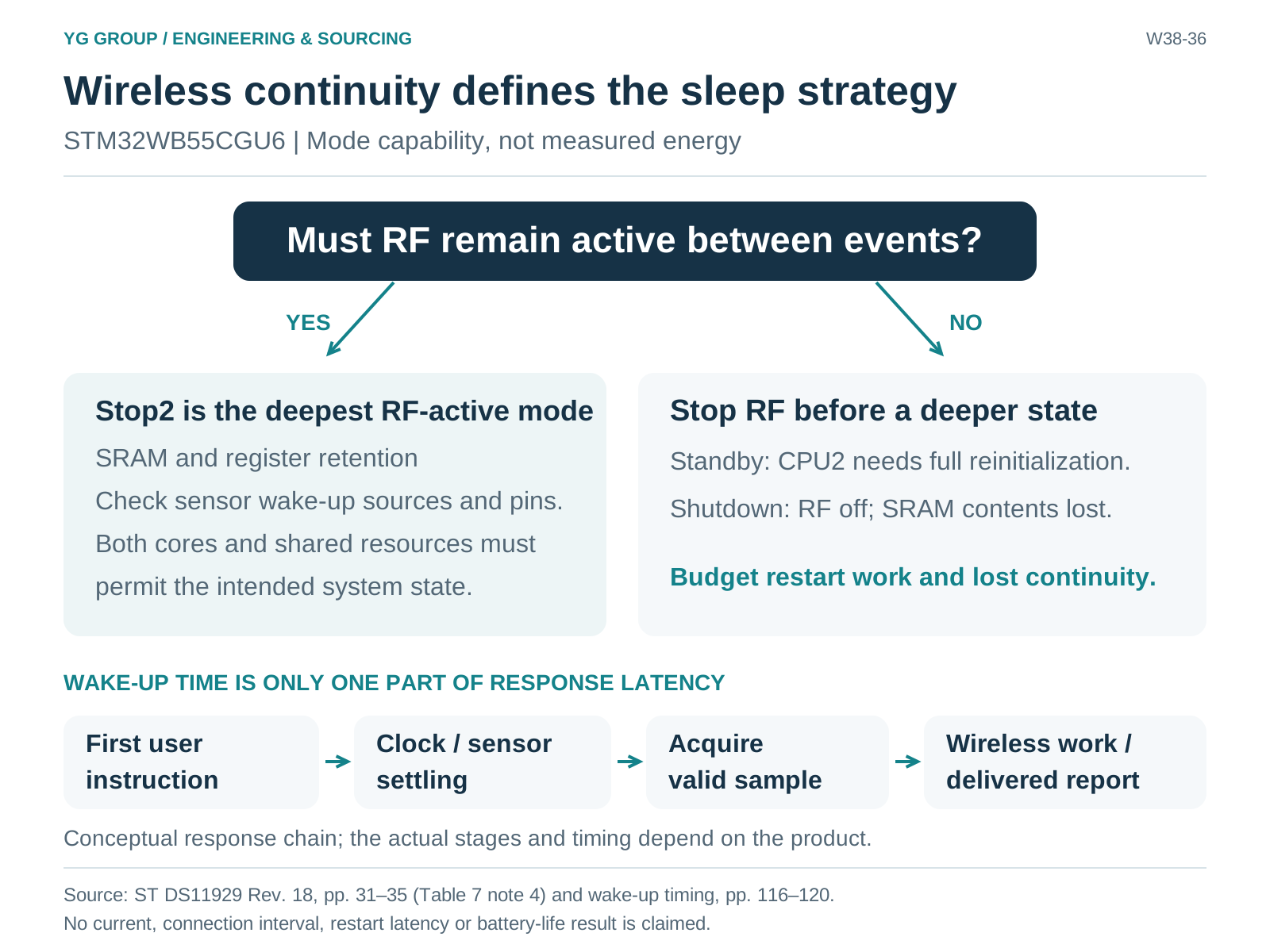
The explicit restriction in DS11929 Table 7 makes Stop2 the deepest mode while RF is active. Entering Standby requires RF to be stopped first, followed by full wireless-processor initialization on wake-up. Account for the resulting loss of continuity and restart work.
It is a Shutdown-mode typical value at VDD = 1.8 V and 25°C, with the RTC disabled and the radio off. It is not the average current of a connected BLE sensor. That average includes wireless events, application work, sensors, and board loads.
It helps only if it reduces the relevant activity without adding other costs. The stack may still schedule radio events, sensors may continue sampling, and reconnect behavior may dominate. Compare complete current traces and response requirements for each configuration.
By Ying Lin
STM32WB55CGU6 combines an application processor, a dedicated wireless processor, and a Bluetooth Low Energy radio in a 48-pin package. For a battery-powered smart home sensor, its useful operating point depends on retained wireless state, sensor activity, and the time between events. This guide explains how to select sleep behavior, build an event-based current budget, and verify the complete board without confusing a datasheet mode current with achievable battery life.
A temperature monitor, a door contact, and a commissioning button can share an MCU while needing different wireless schedules. A temperature monitor may tolerate delayed reports. A door contact may need prompt notification after an edge. A commissioning function may need to remain discoverable only while a user is installing the product. Specify those behaviors before selecting the lowest numbered current in a datasheet.
For each product state, write down what must remain available: the sensor interrupt, a periodic sampling timer, a BLE connection, discoverable advertisements, or retained application data. Also define how the product behaves when its central device is absent. A sensor that spends hours searching for a disconnected hub can have a very different energy profile from the same board in a stable connection.
Use this requirement to separate three schedules: sampling, radio activity, and reporting. They do not necessarily run at the same rate. Firmware can collect samples locally and report only on a meaningful change, provided this still meets the product's freshness and alarm requirements. A longer reporting period alone does not prove that the radio or application processor wakes less often; that must be checked in the actual stack and current trace.
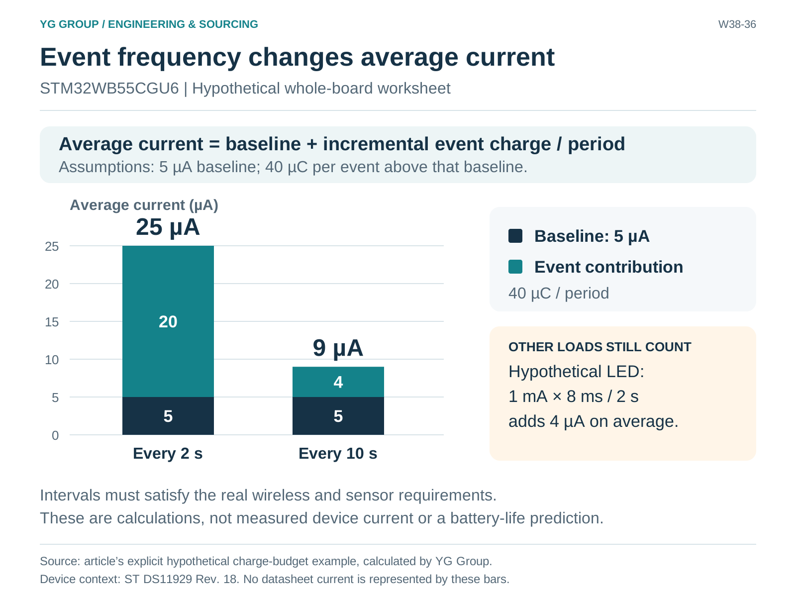
**Figure 1. Wireless continuity defines the sleep strategy.** YG Group synthesis of ST DS11929 Rev. 18 power-mode and wake-up boundaries. Stop2 is the deepest mode while RF is active; Standby requires RF stopped first and CPU2 full initialization on wake. The lower flow is a conceptual response budget, not a measured timing diagram or a guarantee that every listed stage runs in every event. Sources: [supporting source 1](https://www.st.com/resource/en/datasheet/stm32wb55cg.pdf). **Figure 2. Event frequency changes average current.** Hypothetical worksheet from the article, calculated by YG Group: 5 µA + 40 µC/2 s = 25 µA and 5 µA + 40 µC/10 s = 9 µA. Event charge is incremental above baseline. These are not STM32WB55CGU6 measurements, approved BLE timing settings or battery-life predictions. Sources: [supporting source 1](https://www.st.com/resource/en/datasheet/stm32wb55cg.pdf).Not on the same footprint. RGV6 uses a 68-pin VFQFPN package rather than the 48-pin UFQFPN package. Treat it as a board-level design alternative requiring an interface and layout review.
STM32WB55CGU6 is an STMicroelectronics wireless MCU with 1 Mbyte of flash and 256 Kbytes of SRAM. Its application processor is an Arm Cortex-M4 operating at up to 64 MHz; a Cortex-M0+ handles wireless processing. The full ordering code selects the 48-pin UFQFPN package and the −40°C to +85°C ambient temperature grade. The standard VDD operating range is 1.71–3.6 V, with separate conditions for particular supplies and functions. ST datasheet, Table 2 and ordering information.
The exact ST ordering page for STM32WB55CGU6, checked September 20, 2026, identifies a tray-packed, active device. This establishes the orderable identity; it does not establish YG Group availability or a committed delivery date.
Table 1. Package-specific resources that affect a sensor design
| Resource | STM32WB55CGU6 boundary | Design consequence |
|---|---|---|
| Package | UFQFPN48, nominal 7 × 7 mm body | Use the 48-pin pinout and footprint, including its exposed ground pad |
| GPIO | 30 GPIOs in the family resource table | Allocate sensor, debug, oscillator, and interface functions before committing the layout |
| Dedicated wake-up pins | Two package-available WKUP pins | Distinguish deep-mode wake-up pins from general interrupt capability |
| Serial interfaces | Two I2C instances; one SPI instance | Do not transfer the larger package's two-SPI resource count |
| Analog conversion | 12-bit ADC; 13 channels including three internal channels | External channel availability and sampling conditions constrain the sensor interface |
| Capacitive touch | No touch-sensing controller availability for this package | Family-level touch-channel claims do not apply to CGU6 |
| ADC reference connection | VREF+ internally connected to VDDA in UFQFPN48 | There is no separate VREF+ package pin for an independent external reference |
Source: DS11929 Rev 18, Table 2, pin descriptions, and package information. Compiled by YG Group. Peripheral functions share pins; the counts do not imply simultaneous access to every alternate function.
The two processors also share resources. ST provides interprocessor communication and hardware semaphores, while portions of flash and SRAM can be reserved or secured for the wireless processor. Consequently, a 1 Mbyte flash label is not a promise that the application image can consume the entire device. Check the selected wireless image, application linker map, buffers, and update strategy together. ST datasheet, architecture and memory sections, pp. 17–20.
Putting the Cortex-M4 to sleep does not necessarily put the whole chip into its deepest state. The actual system state must satisfy the needs of both cores and their shared resources. A pending wireless operation, peripheral transaction, or software event can keep the system in a shallower state than the application expects.
For a sensor that retains BLE activity between events, Stop2 is the important deep-sleep boundary. The explicit restriction in Table 7 states that Stop2 is the deepest available mode while RF is active. To enter Standby, the application must first stop RF activity; CPU2 requires full initialization on wake-up. This makes Standby a different operating strategy, with restart costs and lost wireless continuity to assess. ST datasheet, power modes and Table 7 footnote 4, pp. 31–35.
Table 2. Match the mode to the job that must survive
| Mode or state | Relevant behavior | Appropriate question for a smart home sensor |
|---|---|---|
| Sleep | Application CPU stops while enabled clocks and peripherals can continue | Is an active transfer or peripheral requirement keeping the board awake? |
| Stop0 / Stop1 | Retention with more peripheral operating or wake-up possibilities than Stop2 | Does the selected interface require this shallower state? |
| Stop2 | SRAM and register retention; deepest mode permitted while RF remains active | Can the application become idle between scheduled wireless and sensor events? |
| Standby | RF must first be stopped; wireless processor must be reinitialized after wake-up | Is the idle period long enough to justify restarting the wireless subsystem? |
| Shutdown | RF is off and SRAM content is lost | Is this a shipping or intentionally disconnected state with a defined restart path? |
Source: ST datasheet, Section 3.9 and Tables 7–8. This table compares capability, not measured product current.
Mode names cannot replace a state-transition test. Have firmware record why it woke, what work it performed, and whether it returned to the intended idle state. A forgotten periodic task can dominate a sensor with infrequent reports. A debug connection or continuous logging can also change the state being measured; record the test configuration and then repeat the measurement with the production configuration.
The datasheet's wake-up timing is the delay from the event to the first user instruction. It is not a promise that a sensor conversion has finished, the external radio clock has settled, or a BLE notification has reached its destination. The end-to-end response budget must include all of those stages that the product actually needs. ST datasheet, Section 6.3.9 and clock characteristics, pp. 116–120.
The datasheet is useful for estimating the scale of individual states. Table 30 gives typical BLE radio consumption at VDD = 3.3 V: at 0 dBm transmit power, 5.2 mA with the SMPS enabled and its feedback voltage at 1.4 V, compared with 8.8 mA in bypass. Receive consumption is 4.5 mA and 7.9 mA respectively under the listed configurations. These figures include the RF subsystem and digital processing. They are not whole-board averages. ST datasheet, Table 30, p. 92.
An event contains more than the transmit plateau. It can include clock startup, application work, sensor settling, conversion, bus transfers, radio preparation, receive windows, packet exchange, and return to sleep. Integrating the current across that complete event gives charge in coulombs. Comparing event charge is usually more informative than comparing the smallest instantaneous reading on a meter.
For a periodic workload, a useful accounting model is:
Average current = baseline current + event charge above baseline / event period
The words “above baseline” prevent double counting. If event charge was measured from zero instead, use a time-weighted calculation that removes the baseline during the event. For multiple event types, add each event's incremental charge multiplied by its frequency, provided the event definitions do not overlap.
Consider a hypothetical worksheet, not an STM32WB55CGU6 measurement. Assume the complete board has a 5 µA baseline and each recurring event contributes 40 µC above that baseline. One event every two seconds adds 20 µA, giving a 25 µA average. One every ten seconds adds 4 µA, giving 9 µA. The arithmetic shows why event frequency matters. It does not establish that either interval satisfies BLE connection parameters, discovery expectations, or the sensor's response requirement.
The same worksheet can expose smaller loads. Suppose an indicator consumes 1 mA for 8 ms every two seconds. Its contribution is 4 µA average, before any MCU work needed to control it. That can be significant next to a few-microamp idle target. This is also an illustrative assumption; measure the actual indicator circuit and duty cycle before adding it to a product budget.
Do not convert the result directly into a marketed lifetime using nominal battery capacity alone. Usable capacity depends on the chosen cell and operating conditions, and brief radio pulses can expose voltage-drop problems before a simple capacity calculation predicts exhaustion. Record battery voltage during the peak event, temperature, source resistance, and the point at which the product can no longer meet its functional requirement.
Sleep-current budgets need temperature limits. In Table 43, the Stop2 row with RTC clocked by the specified LSE crystal in low-drive mode, BLE disabled, and VDD = 3.0 V lists 2.45 µA typical at 25°C and 23.0 µA typical at 85°C. The corresponding characterization-based maxima are 4.31 µA and 58.0 µA. These are device conditions, not a connected sensor's measured average. Their practical lesson is that a room-temperature typical value leaves a substantial part of the budget unexamined. ST datasheet, Table 43 and its footnotes, pp. 104–105.
The operating supply range also needs a functional reading. The device can operate down to 1.71 V under its recommended conditions, but this does not mean the SMPS should remain enabled throughout every battery discharge. Table 24 states that when the minimum VDD is below 1.95 V, SMPS operation must be conditioned by the BORH configuration to force bypass, or the SMPS must not be enabled. The low-voltage power strategy therefore belongs in both firmware and the board validation plan. ST datasheet, Table 24 footnote 2, p. 87.
Measure the transition around the chosen low-battery boundary under load. A design may operate normally at a steady bench supply and reset when an aged or cold cell supplies a radio pulse. The battery, decoupling, power conversion, brownout behavior, and retry policy have to work together. Repeated rebooting or reconnecting can itself increase consumption and accelerate a marginal supply problem.
VBAT is another distinct domain. It can preserve backup functions such as the RTC and backup registers when the main supply is absent; it does not keep the BLE radio operating. Treating the backup pin as a second wireless supply would produce an incorrect circuit and an incorrect power budget. ST datasheet, power distribution and VBAT operation, pp. 25 and 38.
The two I2C instances have different low-power capabilities. I2C3 supports the Stop2 wake-up path described by ST, while I2C1's corresponding operation is limited to Stop0/Stop1. LPUART1 and LPTIM1 also have capabilities relevant to Stop2. These distinctions can affect peripheral selection before the PCB is routed. ST datasheet, Table 7 and peripheral descriptions, pp. 33–35 and 50–53.
However, I2C address-match wake-up is a specific receiving scenario. It does not mean the sleeping MCU autonomously acts as an I2C master, polls a sensor, and processes its result. For a conventional sensor connected to an MCU master, decide whether a timer or the sensor's separate data-ready interrupt wakes the application to start the transaction. Match that interrupt to the selected sleep mode and package-available pin.
Power gating the sensor adds another dependency. Before shutting its rail off, consider pull-ups and signals that remain driven from the MCU domain. Otherwise, the interface can create unintended current paths or keep the sensor partly powered. On wake-up, include the sensor's own startup and settling requirements before accepting a reading. These requirements must come from the selected sensor's documentation and measurements; they cannot be inferred from the MCU's wake-up time.
Analog sensors need the same discipline. STM32WB55CGU6 has a native 12-bit ADC; hardware oversampling does not by itself guarantee 16 effective bits. Source impedance, input capacitance, sampling time, reference behavior, and supply conditions affect the result. On this package VREF+ is tied internally to VDDA, so noise or movement on the analog supply is part of the measurement problem. ST's ADC tables also distinguish channel types and operating conditions. Select a sampling configuration for the actual circuit, then verify settling and accuracy after waking. ST datasheet, Section 3.14 and ADC characteristics, pp. 44–46 and 139–151.
Increasing a divider resistance may reduce its static current while increasing settling time at the ADC input. Turning the divider on only for a reading may reduce average load while adding another transient. Evaluate the complete sample's charge and accuracy together. The on-chip temperature sensor measures die temperature; it should not be treated as a calibrated room-temperature sensor without a separate thermal and accuracy assessment.
The integrated balun reduces part count, but the RF pin still needs the appropriate matching/filtering and antenna implementation. ST's typical RF schematic is an indicative circuit, not proof that an arbitrary sensor PCB and enclosure will produce the same radio behavior. Antenna surroundings and layout changes can affect the link and therefore the number and duration of wireless events. Include the final enclosure and intended installation orientations in validation. ST datasheet, RF front end and typical application, pp. 21–24.
The power schematic must also follow the package-specific connections: VDDRF and VDDSMPS are tied to VDD as specified, local decoupling serves the relevant supply pins, and the exposed pad has the required ground connection. The SMPS network and bypass configuration should be reviewed together with the selected operating range. A small PCB area saving that compromises these connections can cost more in unstable behavior than it saves in component count. ST datasheet, power supply schemes, pp. 25–29 and 81–83.
Review every external load that survives sleep. ST specifically calls out current through pull resistors held at the opposite level and additional input current when digital inputs sit at intermediate voltages. Unused pins need an intentional configuration consistent with the circuit. A continuously enabled battery divider, status LED, sensor heater, or external regulator can overwhelm the MCU's idle current. ST datasheet, I/O system current consumption, p. 113.
Start with a firmware configuration that isolates the intended idle state, then add the real workload in controlled steps. The purpose is to locate consumption, not to present the smallest stripped-down result as product performance.
Table 3. Measurements that turn an estimate into a product budget
| Measurement | What to record | What it resolves |
|---|---|---|
| Idle baseline | Supply, temperature, clocks, retained state, enabled peripherals, debugger state | Whether the MCU and board reach the intended state |
| Sensor transaction | Warm-up, conversion, interface transfer, settling, shutdown | The complete cost of obtaining a valid sample |
| Wireless event | Stack version, connection or advertising settings, payload, power setting, trace duration | Charge per actual event rather than transmitter current alone |
| Normal long capture | Representative sampling and reporting activity | Whether event counts predict the observed average |
| Hub absent / weak link | Search, retries, reconnect behavior, timeout policy | Whether abnormal connectivity dominates the budget |
| Low-voltage and temperature corners | Current plus rail minimum during pulses and functional outcome | Supply margin and temperature sensitivity |
| Reset and update | Recovery time, initialization, update behavior | Infrequent but potentially costly product states |
Source: engineering validation framework compiled by YG Group from the power-mode, current, clock, and interface boundaries in DS11929 Rev 18. These are proposed measurements; no board test results are claimed.
Use measurement equipment and a connection method that resolve both the low baseline and short high-current events without causing excessive supply drop. Integrate over enough cycles to include the slowest recurring work. Preserve the firmware and wireless-stack versions with the trace; a software change can alter event timing even when the BOM stays constant.
For repeat builds, carry the approved oscillator, RF network, sensor, regulator, and battery requirements into the BOM. A replacement that changes startup, leakage, or radio behavior should trigger the relevant part of the power test. This makes a validated energy budget reproducible across engineering changes and production lots.
STM32WB55CGU7 keeps the 48-pin UFQFPN package and raises the specified ambient grade to −40°C to +105°C. It is relevant when the thermal requirement changes. The higher temperature grade does not promise the same leakage at a higher temperature, and it does not eliminate the need to review the complete board.
STM32WB55RGV6 is the 68-pin VFQFPN version, with a nominal 8 × 8 mm body. It exposes more resources, including 49 GPIOs in the datasheet's resource table, but requires a different footprint and pin assignment. It is a design alternative when the sensor platform needs more interfaces; it is not a drop-in replacement for CGU6. ST datasheet, Table 2 and package drawings.
Keep the exact MCU ordering code separate from the installed wireless software identity. The silicon's protocol capability does not establish that a selected firmware image implements every advertised feature or that the finished sensor has completed qualification. Record the actual stack release and required features before freezing the product specification.