
Jolin Zeng




| Picture | Part Number | Manufacturer | Stock | Action |
|---|---|---|---|---|
 | MIC95410YFL-TR | Microchip | 7,640 |
No. Its switched IN path operates up to 5.5 V. The separate VS bias operates from 2.7 V to 9 V, and that higher bias limit does not apply to IN. Use the device only on an appropriate low-voltage branch after any required conversion. It is a load switch, so it does not regulate or step down the incoming voltage. Microchip lists servers as an application, but that does not establish suitability for a specific server architecture or GPU core supply.
A nominal 1.8 V high does not meet the guaranteed CTL high threshold. The datasheet requires at least 2.0 V with VS from 2.7 V to 5 V, and at least 2.4 V with VS above 5 V through 9 V. Check the controller's guaranteed output levels and the permitted CTL voltage relative to VS. An appropriate interface may be necessary. Also define the command during reset, shutdown, and bias loss; a floating CTL input produces an unpredictable state.
No. GC changes the gate-charge behavior and can reduce capacitor-charging inrush during startup. It does not program a regulated fault-current threshold. The familiar estimate using 27 µA times output capacitance divided by GC capacitance describes the second gate-charge stage only. It excludes the initial peak and active load current. A larger GC also changes the duration of transient dissipation, so check the complete voltage-current waveform and safe-operating-area conditions rather than assuming slower is always safer.
By Jolin Zeng
The MIC95410YFL-TR is a low-resistance load switch for a low-voltage power path, with a separate bias supply and an external capacitor that adjusts turn-on behavior. On a server auxiliary rail, it can help control how a downstream capacitor bank is connected and how a load is switched. It does not convert a 12 V bus into a lower voltage, regulate the output, or provide a programmable current-limit threshold.
Microchip lists servers among the device's applications. That supports examining a server auxiliary-rail use case; it does not establish adoption in a particular AI server or suitability for a GPU core supply. The useful design question is narrower: can this switch connect the intended low-voltage load without disturbing the upstream supply, violating its own limits, or leaving the load in an uncertain state during a power transition?
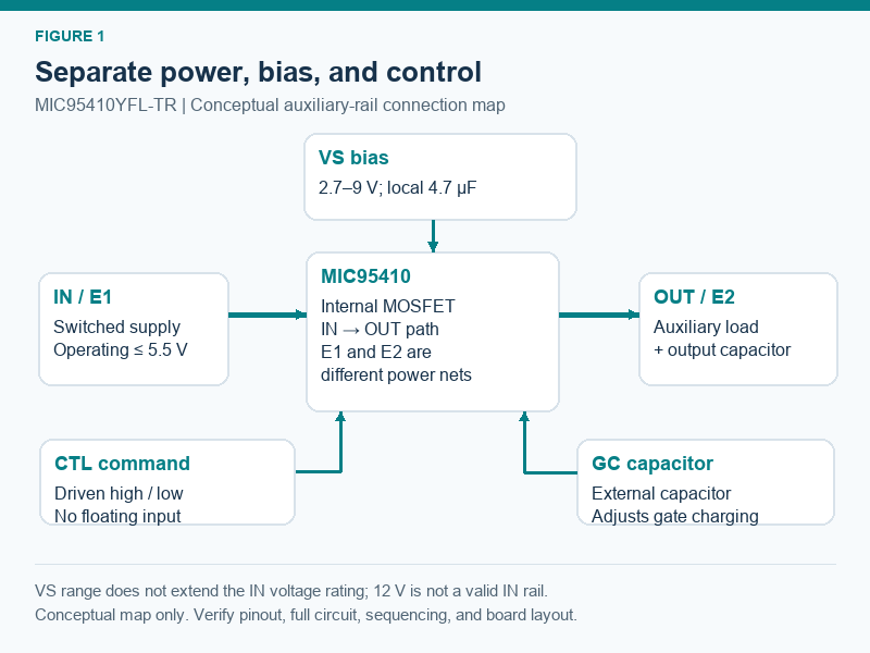
Start by separating the switched power path, the bias supply, and the control input. IN feeds the internal N-channel MOSFET and OUT supplies the load. VS powers the switch's internal circuitry. CTL tells it when to turn on or off. Combining these into one informal “supply” label makes sequencing mistakes harder to spot.
The switched input operates up to 5.5 V and can switch rails below 1 V. The separate VS bias must remain within its 2.7–9 V operating range. The upper VS value is not an allowable voltage for IN. Likewise, the IN absolute maximum is not the recommended operating ceiling. A server's 12 V distribution rail therefore needs an appropriate conversion stage before this device can switch a low-voltage branch. .
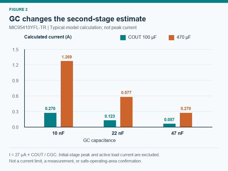
**Figure 1.** Keep the switched IN-to-OUT path separate from the VS bias, CTL command, and GC capacitor. E1 connects to IN and E2 to OUT. This conceptual connection map illustrates the design review; it is not a complete reference schematic or a measured server board. **Figure 2.** Calculated second-stage charging current from I = 27 µA × COUT / CGC. The bars exclude the initial-stage peak and active load current. They are typical-model comparisons, not measurements, guaranteed current limits, or confirmation of safe operating area.Microchip describes a possible floating gate and an unpredictable switch state. Do not assume that loss of bias guarantees a clean off state. Review how CTL is driven as each supply rises and falls, including controller reset and retained control voltages. A default pull-down can help in suitable circumstances, but it is not a universal solution to every power sequence. Validate the relevant state transitions on the actual board and address unintended supply paths through other connected circuits.
No. Check conduction loss, actual copper paths, ambient temperature, and transient startup stress. The datasheet's on-resistance figures have stated bias/input and test-current conditions; its junction-to-ambient thermal resistance is tied to an evaluation-board condition. Neither can be transferred blindly to a compact customer PCB. The two exposed pads are also different power nets: E1 is IN and E2 is OUT. They must not be connected as though both were ground thermal pads.
Start with the missing system function. TPS22990DMLR offers a 10 A comparison with power good; TPS22992RXPR offers a compact 6 A option with status and thermal shutdown, but it is not the S version with additional short-circuit protection. TPS22965DSGR and TPS22975DSGR provide other 6 A comparisons, with feature differences including thermal shutdown for TPS22975. Recheck bias, control, timing, discharge, package, and layout requirements. None is established here as a drop-in replacement.
Table 1. The connections have different electrical jobs.
| Connection | Device function | Design check |
|---|---|---|
| IN, pins 2 and 3, exposed pad E1 | Switched supply entering the power MOSFET | Keep the operating rail at or below 5.5 V and review input transients. |
| OUT, pins 6, 7, and 8, exposed pad E2 | Switched supply delivered to the load | Include load capacitance, steady current, and possible external back-power paths. |
| VS, pin 5 | Internal bias supply | Provide 2.7–9 V and the recommended local 4.7 µF ceramic bypass. |
| CTL, pin 10 | Active-high on/off command | Drive valid levels and define behavior during reset and bias transitions. |
| GC, pin 9 | External gate-control capacitor connection | Choose capacitance for the startup behavior, then check the actual waveform. |
| GND, pin 4 | Circuit reference | Keep the local bypass and control references well defined. |
| NC, pin 1 | No internal connection | Microchip recommends connecting it to IN to widen the input trace. |
The exposed pads require attention early in layout. E1 belongs to IN and E2 belongs to OUT. They are not two interchangeable ground pads, despite their location beneath a small package. A footprint created by copying a generic exposed-pad component can therefore cause a serious connection error. Review the manufacturer's pin diagram and recommended land pattern together with the schematic net assignment.
For a conceptual 3.3 V auxiliary branch, IN might come from an upstream converter while VS comes from an appropriate bias supply. That arrangement is only an example: the real architecture determines which source appears first, how long it remains valid, and what happens during shutdown. Record those relationships in the power-state description before choosing a gate-control capacitor.
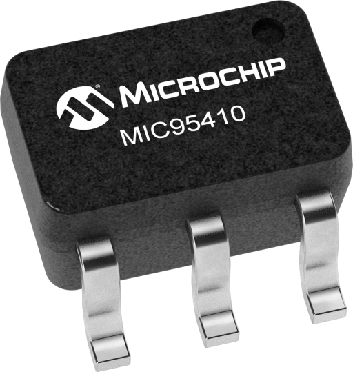
The complete orderable part number also matters. MIC95410YFL-TR identifies the temperature/package option and the tape-and-reel ordering arrangement shown in Microchip's product identification system. The TR option is listed as a 5,000-piece reel; the T5 packing option is not a different electrical alternative. The package itself carries an abbreviated marking, so procurement and footprint records should retain the full code. Product identification system, page 19.
A controller output that is described only as “logic high” is not enough. The MIC95410's CTL thresholds depend on the bias range. The datasheet specifies a high level of at least 2.0 V for VS from 2.7 V to 5 V, and at least 2.4 V for VS above 5 V through 9 V. The low range is 0–0.8 V. A nominal 1.8 V GPIO does not meet either guaranteed high threshold.
Check the controller's guaranteed output level under its actual loading and supply conditions, including reset behavior. A level translator or other appropriate interface may be needed. Also check the maximum permitted input level relative to VS. A control signal that stays high after the bias rail has disappeared needs a deliberate design review, not an assumption that digital inputs remain harmless under every supply sequence.
Table 2. Control and bias cases that belong in the sequence review.
| Condition | Documented behavior or limit | Required design action |
|---|---|---|
| VS = 2.7–5 V | CTL high requires at least 2.0 V | Verify the controller's guaranteed high output. |
| VS above 5 V through 9 V | CTL high requires at least 2.4 V | Recheck interface margin at the higher bias range. |
| CTL = 0–0.8 V | Defined low input range | Ensure reset and shutdown can establish a valid low. |
| CTL left floating | Switch state is unpredictable | Provide a defined drive or an appropriate default-state arrangement. |
| CTL high while VS falls to zero | Gate can float and the switch state is unpredictable | Sequence the control and bias deliberately; validate abnormal shutdown cases. |
| Ordinary turn-off | Internal gate discharge and output discharge paths act | Verify output decay against the actual capacitance and external connections. |
Microchip explicitly warns that leaving CTL floating produces an unpredictable state. It also describes an important bias-loss case: with CTL high and VS reduced to zero, the MOSFET gate can float. Do not describe that condition as a guaranteed safe shutdown. A pull-down can help establish a default command when its driving source releases the node, but it does not automatically solve every combination of back-powering, retained control voltage, and collapsing bias.
Write the intended states in plain language: bias valid with the branch off; input available while the controller is in reset; normal turn-on; commanded turn-off; input loss; and bias loss. For each state, identify what drives CTL and whether the downstream circuitry can receive power through another connection. This exercise often reveals a problem that would be invisible in a single steady-state schematic.
The datasheet's turn-off delay also needs careful interpretation. Its timing definition measures from the falling CTL edge to the point where the falling output reaches 90% of the input voltage. That is the beginning of the output's decline, not confirmation that a capacitor bank has discharged to a safe or logic-low voltage. If the system requires a rail below a particular threshold before another action, define and measure that threshold directly.
The external GC capacitor changes how quickly the internal MOSFET gate is charged. Slowing the output rise can reduce the capacitor-charging current presented to the upstream rail. That is useful when several auxiliary loads share a converter and one newly enabled branch must not pull its neighbors out of regulation.
Begin with the downstream capacitance that the switch actually sees. Include discrete capacitors, modules, and any other effective capacitance connected behind OUT. Keep a separate estimate of the active load current during startup. A processor, controller, or peripheral may begin drawing current before the rail reaches its final voltage, so total switch current is not necessarily just capacitor charging current.
The MIC95410 has a two-stage gate-charge behavior. Microchip describes an initial stronger current followed by a lower gate-drive current as the gate-control node rises. For the second stage, the datasheet gives the approximation that charging current equals second-stage gate current multiplied by output capacitance and divided by GC capacitance. The typical second-stage value used in its example is 27 µA. Application information, pages 10–12.
For 100 µF behind the switch and 10 nF at GC, that approximation gives 0.27 A. Increasing GC to 22 nF gives about 0.123 A; 47 nF gives about 0.057 A. These numbers are useful for an initial comparison. They are not guaranteed peak currents, programmed current limits, or complete startup predictions.
Table 3. Illustrative second-stage capacitor-charging current.
| Assumed output capacitance | GC capacitance | Calculated current using 27 µA | How to use the result |
|---|---|---|---|
| 100 µF | 10 nF | 0.270 A | Starting estimate for the lower-current gate-charge stage. |
| 100 µF | 22 nF | 0.123 A | Compare a slower startup candidate under the same assumptions. |
| 100 µF | 47 nF | 0.057 A | Check whether the longer rise is acceptable to the load. |
| 470 µF | 10 nF | 1.269 A | Larger capacitance raises the estimated charging current. |
| 470 µF | 22 nF | 0.577 A | Still excludes initial-stage peak and active load current. |
| 470 µF | 47 nF | 0.270 A | Similar estimate to 100 µF with 10 nF, under this model only. |
Every entry is calculated from the same typical-value approximation. Capacitor tolerance, effective capacitance, operating voltage, and the switch's actual behavior can move the observed waveform. The first stage can produce a higher initial current, and at low input voltage that stage can dominate the transition. Applying the second-stage equation to the entire turn-on event would miss the behavior that may matter most to the upstream converter.
A slower ramp also changes how long the MOSFET carries current with a substantial voltage across it. That creates a transient dissipation question. It is therefore possible to reduce the upstream current peak while making the switch's startup stress more demanding in another way. Review the voltage-current trajectory and duration against the manufacturer's safe-operating-area guidance and the intended thermal conditions.
Do not translate “adjustable slew rate” into “short-circuit protection.” GC shapes gate charging; it does not set a regulated current threshold that safely handles any downstream fault. If the architecture requires a bounded fault current, timed fault response, or circuit-breaker behavior, identify a device or upstream protection strategy that explicitly provides it. The MIC95410's low on-resistance does not provide that function by itself.
A practical development sweep starts with several GC values around the calculated candidate. For each, capture input voltage, output voltage, CTL, and branch current with sufficient bandwidth and a suitable current measurement method. Watch both the initial peak and the slower part of the ramp. Repeat under the most relevant load, capacitance, input-voltage, and temperature conditions, rather than accepting a single pleasant-looking waveform.
Use the upstream converter's behavior as part of the acceptance criterion. The desired result may include a maximum rail droop, a limit on disturbance to another branch, a minimum monotonic output rise, or a maximum startup interval. State those criteria before adjusting GC. Otherwise it is easy to optimize the appearance of the current trace while overlooking whether the downstream load actually starts reliably.
Consider a hypothetical auxiliary module with a 100 µF effective input capacitance. The second-stage estimate for 10 nF at GC is 0.27 A, but suppose the module also begins drawing current partway through the rise. The observed branch current then contains both capacitor charging and the module's demand. If the trace exceeds 0.27 A, that alone does not show that the switch or equation is wrong. First locate the initial gate-charge stage and the point where the load becomes active, then compare the relevant interval with the approximation.
The upstream rail must supply that complete current, so the system acceptance criterion remains based on the measured total. Separating the causes helps choose the correction. More GC may reduce part of the charging demand; a later load-enable command may change active demand; a stronger upstream source may improve rail stiffness. These are different design decisions. Changing the capacitor repeatedly without understanding the current's components can produce a slow startup that still disturbs the shared rail.
If several auxiliary branches use similar switches, repeat the analysis for the allowed combinations of enable commands. Staggered firmware startup can reduce coincident demand only while firmware controls the sequence as intended. A reset path, maintenance mode, or recovery routine may enable branches differently. Include those legitimate operating paths in the sequence review, and avoid relying on a nominal delay that is absent during the very recovery event the system must tolerate.
Once the switch is on, conduction loss is approximately load current squared times on-resistance. The datasheet gives 6.6 mΩ typical and 9.9 mΩ maximum on-resistance under its listed bias/input conditions at a 4 A test current. A screening calculation at 7 A using 9.9 mΩ gives about 0.485 W. The arithmetic is straightforward; deciding whether the board can dissipate that heat requires more information.
The 7 A headline is not an unconditional current guarantee for any footprint, copper area, ambient temperature, or enclosure. The operating junction-temperature limit is 125°C. The stated 60°C/W junction-to-ambient value is associated with the manufacturer's evaluation-board condition in still air. Treat it as a documented reference condition, not a measured thermal resistance for the customer's PCB. Electrical and thermal characteristics, pages 4–5; layout guidance, pages 11–12.
If that 0.485 W screening loss were combined with 60°C/W, the estimated junction rise would be about 29°C. This conditional example is useful for judging scale. It does not establish a final temperature, because on-resistance, actual operating conditions, copper spreading, and neighboring heat all matter. Keep the 4 A resistance test condition visible when using its value in a 7 A estimate, and validate the intended high-current use on the real board.
Heat leaves the device substantially through the IN and OUT connections and their associated exposed pads. Widen those traces promptly and provide adequate copper paths, consistent with the manufacturer's layout guidance and the board's electrical constraints. Suitable plane connections and vias can help spread heat, but the two exposed pads must remain on their correct power nets. A large ground pour connected to the wrong pad is not a thermal improvement.
Place the VS bypass close to the device and make its return path short and clear. Keep the GC capacitor connection compact as well. Long, noisy control paths make startup behavior harder to reproduce and debug. High-current routing should be reviewed for voltage drop and heating beyond the component itself: connectors, vias, narrow necks, and return paths can limit the branch before the switch's nominal current rating becomes relevant.
Check the transient case separately from steady conduction. During turn-on, the switch can see both substantial current and a large IN-to-OUT voltage. A small final I-squared-R loss does not describe that interval. The datasheet's safe-operating-area information concerns transient operation; it should not be turned into a general DC operating promise or reproduced without its conditions.
Turning CTL low starts more than one internal action. The gate-control node is pulled down, and the output has an internal discharge path. The discharge network includes resistance and a diode; its behavior is not the same as an ideal resistor directly connected from OUT to ground over the entire voltage range.
The electrical table lists a typical discharge resistance of 2.3 kΩ at a 5 V output, with different typical values at lower output voltages. A large capacitor bank can therefore remain charged well after the switching delay has elapsed. The active load may speed the decay, while another powered interface may sustain it. Measure the voltage at the point whose state matters to the system, rather than assuming that an off command immediately removes all energy.
Back-powering deserves its own review on an auxiliary branch. Signals, pull-ups, protection structures in connected devices, and other supply connections can feed a nominally disabled load. Do not assume reverse-current blocking or complete isolation unless the relevant behavior is explicitly established for the circuit. A switch controlling the main rail does not automatically control every possible path into a peripheral.
Table 4. Observations to collect during board validation.
| Test situation | Observe | Decision the result supports |
|---|---|---|
| Normal enable | CTL, VS, IN, OUT, and branch current | Confirm valid control and acceptable startup at the chosen GC. |
| Largest intended capacitance | Initial current peak, slower ramp, upstream droop | Check source disturbance and transient switch stress. |
| Minimum intended input rail | Output rise and current waveform | Determine whether first-stage behavior changes the startup assumption. |
| Maximum continuous load | Voltage drop and temperature after settling | Confirm current-path and thermal margin on the actual PCB. |
| Commanded disable | Output decay to the required system threshold | Establish when the downstream load is truly below that threshold. |
| Bias loss and controller reset | CTL and OUT throughout the transition | Identify floating or retained-on conditions that need architectural changes. |
| Other interfaces powered | Disabled-rail voltage and current paths | Find back-powering that the main switch alone cannot remove. |
Keep measurement limitations in the report. Probe loading can matter at GC, and current measurement hardware can add resistance or inductance to a low-voltage branch. State the probe arrangement and bandwidth that matter to the observation. A waveform is more useful when another engineer can reproduce the setup than when it is simply labeled “inrush passed.”
Also distinguish a nominal startup test from a fault test. Repeatedly shorting the output is not a substitute for reviewing whether the architecture has a suitable current-limiting mechanism. If fault behavior must be tested, define the source limits, fixture, energy, measurement plan, and acceptance criteria through the appropriate engineering process. Protective behavior should be established by evidence, not inferred from the presence of a MOSFET.
After selecting GC, retain the value and tolerance in the approved configuration along with the output-capacitance range. A later module change that doubles the capacitance can invalidate the earlier startup result without changing the switch itself. The same applies when firmware changes the enable order or allows several branches to start together. Sequence, capacitance, and upstream source capability are connected design inputs.
A shutdown acceptance test should also use a system-defined endpoint. For example, a peripheral may need its supply to fall below its own reset threshold before a restart can be considered a fresh power cycle. That threshold and any minimum off time come from the peripheral's requirements, not from the MIC95410's turn-off-delay number. Measure the rail through the entire decay, including any plateau caused by another interface, and check that the controller waits for the required condition.
Record whether the test begins with an active load or an idle one. An active load may discharge the capacitor quickly during development, while an idle or disconnected module decays more slowly in service. Testing both relevant states can explain an intermittent restart failure without blaming the load switch for behavior the initial test never covered. Keep the result tied to the tested configuration rather than describing it as a universal discharge time.
Compare a related load switch against a specific requirement: more continuous-current capability, a power-good output, thermal protection, a different bias arrangement, or a smaller package. Package size and on-resistance alone cannot establish equivalence. The following official orderable-part pages support a first screening comparison, with detailed design qualification still required for any change.
Table 5. Four related load switches for a deliberate redesign comparison.
| Exact related MPN | Manufacturer | Useful comparison point | Important boundary |
|---|---|---|---|
| TPS22990DMLR | Texas Instruments | 10 A class, adjustable rise time, power good, output discharge, 10-pin WSON | Different package and supply/bias requirements; review the complete operating envelope. |
| TPS22992RXPR | Texas Instruments | 6 A class, adjustable rise time, power good, discharge, thermal shutdown, 8-pin WQFN-HR | This is the non-S device; do not assign TPS22992S short-circuit protection to it. |
| TPS22965DSGR | Texas Instruments | 6 A class, adjustable rise time and output discharge, 8-pin WSON | Lower current class than the MIC95410 headline and a different pinout/package. |
| TPS22975DSGR | Texas Instruments | 6 A class, adjustable rise time, discharge and thermal shutdown, 8-pin WSON | Reassess load current, control behavior, protection needs, and board layout. |
The TPS22990 comparison is useful if the project needs a higher current class and a power-good signal. Its official page lists a 2.5–5.5 V bias range and a switched-input relationship to that bias. Those conditions differ from the MIC95410's separate 2.7–9 V bias range. A feature that looks attractive in isolation still has to fit the available rails. TPS22990DMLR product information.
The TPS22992 option is useful for a more compact branch with status and thermal protection, provided that 6 A is sufficient. The family includes a separate S version with additional short-circuit protection. Retaining the exact TPS22992RXPR identity prevents a family-page feature from being silently transferred to the wrong orderable device. TPS22992RXPR product information.
TPS22965DSGR and TPS22975DSGR both provide a 6 A comparison in an 8-pin WSON package. Their feature sets differ, including the thermal-shutdown feature highlighted for TPS22975. Compare the protection function actually needed, then inspect detailed timing, discharge behavior, bias requirements, and layout before changing the schematic. Neither is a substitute selected merely by matching a low-resistance headline. TPS22965DSGR, TPS22975DSGR.
All four comparisons require a board and sequence review. A different device may change the capacitor used to set rise time, the relationship between control and bias, the output-discharge behavior, or the status signals available to firmware. Those changes belong in the engineering change record as well as the component comparison.
A useful MIC95410YFL-TR design record states the switched rail, the VS source, the CTL interface, the selected GC value, the allowed output-capacitance range, and the validated continuous load. It also records the accepted startup disturbance and the measured shutdown threshold timing. That information lets a future engineer assess a module or firmware change without guessing why the original circuit worked.
For a server auxiliary rail, the central tradeoff is practical: enough control over startup to protect the shared source, while preserving reliable load startup and acceptable transient stress in the switch. The second-stage equation gives a starting estimate. The full waveform, thermal review, and power-state behavior determine whether the implementation meets the actual system requirement.