Kelsey Lee




No. It contains two N-channel and two P-channel MOSFETs with separate gate connections. The complete rectifier needs suitable external gate control. Body-diode conduction and an assumed automatic startup sequence are not substitutes for a verified controller and circuit that support the chosen P/N topology.
A conducting path contains one N-channel and one P-channel device. At the specified ±10 V gate conditions and 25°C, typical values are 85 mΩ and 161 mΩ, giving 246 mΩ. The listed maxima sum to 300 mΩ. Use the correct temperature and drive conditions; typical values do not establish worst-case heating.
No. The N-channel devices have a +100 V drain-source rating, while the P-channel devices have a −80 V rating. Check polarity and magnitude for each device and every transient. A TVS standoff voltage alone does not establish that its actual clamping voltage remains below the P-channel limit.
By Kelsey Lee | YG GROUP
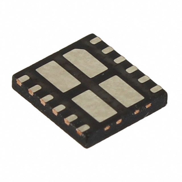
FDMQ8203 combines two N-channel and two P-channel MOSFETs for a compact bridge power path. With suitable external gate control, its channel conduction can dissipate less power than an assumed two-diode path at a defined current. The device still has nonzero resistance and contains no autonomous rectifier controller. Its different N/P voltage ratings, gate limits and exposed drain connections must be checked as part of the complete PoE powered-device front-end.
A conventional diode bridge has two forward-biased diodes in the conducting path. An appropriately controlled MOSFET bridge can carry current through channels with a resistive drop instead. That distinction can reduce heat in a powered-device front-end, but it does not eliminate rectifier loss. The benefit depends on load current, gate drive, device temperature and the losses of the complete control implementation.
FDMQ8203 contains four transistors: Q1 and Q4 are N-channel, and Q2 and Q3 are P-channel. It is a MOSFET array, not an autonomous ideal-diode controller or a complete PoE interface. The four gates remain separate pins. Select and verify a control circuit suited to that mixed P/N arrangement, including startup, polarity changes and periods when the gates are not driven.
At 25°C and the stated gate-drive conditions, the typical N-channel on-resistance is 85 mΩ and the typical P-channel value is 161 mΩ. Their sum is 246 mΩ for one conducting bridge path. The corresponding listed maximum values sum to 300 mΩ. Doubling only the N-channel value misses the P-channel resistance and understates conduction heat.
No. The exposed drain areas are electrically active. They form the two shared drain groups D1/D2 and D3/D4, associated with the bridge AC-input nets. Respect the physical pad drawing and electrical grouping. Treating the underside as one grounded thermal pad can short the bridge nodes.
Table 1. N-channel plus P-channel conduction resistance | Source: manufacturer documents in References; assumptions and operating conditions are stated in the table or adjacent text. Compiled / calculated by: YG GROUP.
| Resistance basis | N-channel | P-channel | One N+P path |
|---|---|---|---|
| Typical, 25°C, stated ±10 V gate drive | 85 mΩ | 161 mΩ | 246 mΩ |
| Listed maximum, 25°C, same gate conditions | 110 mΩ | 190 mΩ | 300 mΩ |
| Typical, 125°C, stated gate conditions | 147 mΩ | 273 mΩ | 420 mΩ |
For an editorial calculation, assume 0.6 A load and use the 25°C typical path resistance. P_FET = I²R = 0.6² × 0.246 = 0.08856 W. If each of two comparison diodes is assumed to drop a constant 0.6 V, P_diode = 2 × 0.6 × 0.6 = 0.720 W. The calculated difference is 0.63144 W. These numbers illustrate the mechanism; they are not measured efficiency or a guaranteed saving for a specified diode part.

Figure 1. Calculated conduction-only comparison: I²R using typical N+P path resistances of 0.246 Ω at 25°C and 0.420 Ω at 125°C, at the datasheet’s specified ±10 V gate conditions, versus an assumed constant 0.6 V drop per diode. At 0.6 A the 25°C calculation is 0.0886 W versus 0.720 W. Controller, switching and other system losses are excluded; these are not measurements. Source: manufacturer documents in References; calculation / diagram: YG GROUP.
Figure 1 includes the higher typical resistance at 125°C to show the sensitivity to temperature. A real diode’s voltage also changes with current and temperature, and the external gate controller consumes power. Switching, wiring and downstream conversion losses remain outside this comparison. Do not convert the conduction-only curves into a whole-PD efficiency claim or an enclosure-temperature reduction without additional evidence.
The N-channel devices are rated at +100 V drain-source; the P-channel devices at −80 V. The lower magnitude is an important boundary for the bridge. The nominal PoE supply does not describe every surge at the device terminals. Check each transistor’s drain-source polarity, gate-source stress and transient waveform in all input orientations and during startup.
A TVS marked with a suitable standoff voltage can still clamp above a transistor’s rating at the actual pulse current. Protection selection requires the rated clamping behavior, waveform, source impedance and layout inductance. Gate protection must likewise account for the source node moving with input polarity.
Current ratings have specific thermal conditions. The package headline current at a controlled case temperature is not a blanket continuous-current allowance for any compact PCB. Use the per-device operating conditions and total power-path dissipation. Compliance with a PoE standard belongs to the complete interface, including detection, classification, inrush, protection and isolation requirements where applicable; the array alone does not establish that compliance.
The package is a 5 × 4.5 mm WDFN-12, CASE 511CS. Pins 1, 4, 9 and 12 are G1, G2, G3 and G4. The source pins are grouped in pairs: 2/3 for S1, 5/6 for S2, 7/8 for S3 and 10/11 for S4. The bridge outputs connect to the sources, while the shared drain groups connect to the AC inputs.
Table 2. Bridge package and electrical connections | Source: manufacturer documents in References; assumptions and operating conditions are stated in the table or adjacent text. Compiled / calculated by: YG GROUP.
| Connection | Bridge role | Layout consequence |
|---|---|---|
| D1/D2 exposed drain group | AC1 input | Keep this live copper isolated from other bridge nets |
| D3/D4 exposed drain group | AC2 input | Do not merge with AC1 or a ground plane |
| S2/S3, P-channel sources | Positive DC output | Size and route for the actual path current |
| S1/S4, N-channel sources | Negative DC output | Establish the controller’s correct voltage reference |
| G1–G4 | Four external control connections | Verify each gate-source voltage and control sequence |

Figure 2. Electrical bridge concept: Q1/Q4 are N-channel, Q2/Q3 are P-channel, and each gate requires suitable external control. The four physical exposed drain areas belong to two drain nets, D1/D2 and D3/D4, connected to the AC inputs. They are not a common ground pad. This is a functional net drawing, not a fabrication footprint. Source: FDMQ8203/D pin and package diagrams.
The underside contains four physical exposed drain areas grouped into two electrical nets. It is not one ground-connected heat slug. Figure 2 emphasizes electrical connectivity rather than claiming to be a manufacturable land pattern. Build the footprint from the exact package drawing, with the correct pad segmentation and isolation. Thermal vias or copper expansion must preserve those nets; adding a shared ground region under every exposed area would create a short circuit.
The datasheet’s thermal resistance depends strongly on its test board. One condition uses a one-square-inch, two-ounce copper pad on a stated FR-4 board; the minimum-pad condition has a different result. Those test conditions do not establish the assembled product’s thermal resistance or temperature improvement. Model the intended copper and measure the assembled front-end under its representative load and ambient conditions.
LT4321IUF#PBF is a concrete comparison for a different implementation. Analog Devices describes a dual ideal-bridge controller using eight external N-channel MOSFETs. It provides a controller architecture for two bridges; it is not a replacement for the FDMQ8203 array and is not presented as directly driving this mixed N/P device.
That comparison changes both the gate-control strategy and the power-device BOM. Assess the completed circuit’s startup, sensing, component ratings, placement and cost. An all-N topology can be considered when its controller and external MOSFETs fit the requirements. A compact P/N array can be considered when a verified control implementation and its voltage margins fit. The shared goal is lower qualified rectifier dissipation, with accurate connections and nonzero losses made explicit.