
Kelsey Lee



9 views

| Picture | Part Number | Manufacturer | Stock | Action |
|---|---|---|---|---|
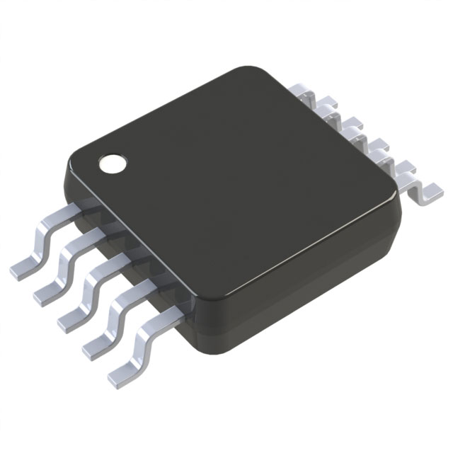 | AD7685ARMZRL7 | Analog Devices | 1,510 | |
| AD7685CRMZRL7 | Analog Devices | 6,350 | |
 | AD7685ACPZRL7 | Analog Devices | 6,240 |
Its exact A-grade row specifies a 15-bit no-missing-code guarantee and ±6 LSB maximum INL. The conversion result is 16 bits. Use the exact grade row rather than the family headline.
The reviewed specification limits the lower VDD range to 200 kSPS. The 250 kSPS limit is associated with VDD from 4.5 V to 5.5 V and the applicable timing conditions.
No. It provides an example network. Its simple RC time constant does not include the complete amplifier, switched ADC load, multiplexer, parasitics, and required error band.
No. This article addresses the test-and-measurement design problem. A component application listing does not establish medical-system certification, patient protection, or the performance of a finished instrument.
AD7685ARMZRL7 is an Analog Devices 16-bit SAR ADC whose input driver must settle before each conversion begins. In a multiplexed test instrument, the demanding case is often a large channel-to-channel step, followed by only a short acquisition interval. The exact A-grade part also has different linearity and no-missing-code guarantees from higher grades. A sound design budgets driver settling, reference recovery, and converter error separately.
The AD7685 family description highlights 16-bit resolution and the best linearity offered by the family. The exact ordering code in this article is AD7685ARMZRL7: A grade, 10-lead MSOP, with a 1,000-piece reel in the reviewed ordering guide. Its specified temperature range is −40°C to +85°C.
The grade distinction changes an instrument's guaranteed performance. A grade has a maximum INL of ±6 LSB and a 15-bit no-missing-code guarantee. It still produces a 16-bit conversion result; output word length, linearity, and no-missing-code resolution are different specifications. The ±2 LSB maximum INL on the family front page belongs to C grade, not to this exact A-grade model. AD7685 Rev. D datasheet, pp. 3 and 27
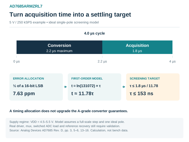
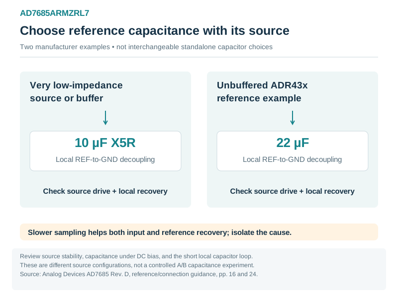
**Figure 1. AD7685ARMZRL7 acquisition window and first-order settling allocation.** Timing example at VDD = 5 V within the 4.5–5.5 V regime: 4.0 µs minimum cycle minus 2.2 µs maximum conversion leaves 1.8 µs acquisition. For an ideal full-scale, single-pole response, allocating half a 16-bit LSB (7.63 ppm) to settling gives t ≈ 11.78τ and τ ≤ 153 ns. This selected error allocation is not an ADC specification, an A-grade accuracy guarantee or proof that an actual driver settles. Sources: [supporting source 1](https://www.analog.com/media/en/technical-documentation/data-sheets/ad7685.pdf). **Figure 2. AD7685ARMZRL7 reference decoupling depends on source topology.** Two distinct manufacturer reference-drive examples: a very low-impedance source or buffer with 10 µF X5R local decoupling, and the unbuffered ADR43x example with 22 µF. Select capacitance together with source drive, stability, DC-bias behavior and the local loop. A longer sample period gives both the input network and reference more recovery time, so an improvement at lower sample rate does not identify the input driver as the cause. No reference circuit is qualified here. Sources: [supporting source 1](https://www.analog.com/media/en/technical-documentation/data-sheets/ad7685.pdf).| Exact ordering model | Maximum INL | No-missing-code guarantee | Package and reviewed reel quantity |
|---|---|---|---|
| AD7685ARMZRL7 | ±6 LSB | 15 bits | 10-lead MSOP; 1,000 |
| AD7685CRMZRL7 | ±2 LSB | 16 bits | 10-lead MSOP; 1,000 |
| AD7685ACPZRL7 | ±6 LSB | 15 bits | 10-lead LFCSP; 1,500 |
The C-grade MSOP part is a comparison candidate when the linearity requirement is tighter. The A-grade LFCSP option changes the package and footprint while retaining the cited A-grade limits. Neither comparison removes the need to review the complete application and controlled BOM.
Start the design budget with those exact limits, then add the external signal-chain errors. A driver that settles to a fraction of an LSB is useful because it avoids adding a large dynamic error. It does not transform A-grade converter linearity into the C-grade guarantee.
The AD7685 samples the difference between IN+ and IN− when CNV rises. The allowed signal span is 0 V to VREF, with IN− acting as a ground-sense input rather than an unrestricted differential signal input. The specification table limits IN− to approximately ground, −0.1 V to +0.1 V under its stated conditions. A bipolar instrument input therefore needs a suitable external scaling and offset circuit; it cannot simply be connected across the two ADC inputs.
During acquisition, the internal sampling network connects to the signal source. The datasheet's simplified model includes a typical 3 kΩ internal resistance and a typical 30 pF sampling capacitance, together with pin capacitance. During conversion, the sampling switch opens. The input is therefore a switched load, not a static resistor or an ordinary high-impedance voltmeter input. AD7685 datasheet, pp. 8 and 13–15
That distinction matters most after an external multiplexer changes channel. The amplifier may have to recover from a large step, charge an external filter capacitor, and then replenish the ADC sampling network before the next CNV edge. Source resistance, multiplexer resistance, amplifier output impedance, filter values, and parasitic capacitance all participate.
The datasheet's typical THD-versus-source-resistance plot illustrates another consequence: a source that looks adequate for a slowly changing DC measurement may give worse distortion for a higher-frequency signal. Use the actual signal bandwidth and error requirement when deciding whether direct drive is acceptable.
The maximum sample rate depends on VDD. At VDD from 4.5 V to 5.5 V, the timing table gives a minimum 4 µs cycle, a maximum 2.2 µs conversion time, and a minimum 1.8 µs acquisition time. At the lower supply range, the cycle is 5 µs minimum and conversion time is 3.2 µs maximum, retaining the 1.8 µs minimum acquisition interval. Thus a 3.3 V design should use the 200 kSPS limit, not automatically copy the 250 kSPS family headline. AD7685 datasheet, pp. 3 and 5–6
For a 5 V, 250 kSPS example, the worst-case converter timing leaves:
4.0 µs cycle − 2.2 µs maximum conversion = 1.8 µs acquisition
That interval is a timing requirement, not a promise that every external amplifier will settle within it. If an external channel changes late in the cycle, its available settling time can be shorter. If it changes during conversion, the driver and external filter can begin moving earlier, but the internal sampling capacitor reconnects only when acquisition begins. Check both events.
Draw the actual sequence around CNV: channel selection, multiplexer propagation, amplifier slew and recovery, ADC acquisition, conversion, and data readback. The sample represents the input at the CNV edge, not at the end of the later SPI transaction. A correct serial word can therefore contain a settling error established before conversion started.
For an ideal single-pole response to a full-scale step, the remaining fractional error is exp(−t/τ). If the design allocates half of one 16-bit LSB to settling, the required fractional error is 1/131072, approximately 7.63 ppm. The corresponding settling interval is approximately:
t = ln(131072) × τ ≈ 11.78 × τ
Using a 1.8 µs interval gives an illustrative time-constant target of about 153 ns or less. This is a deliberately chosen engineering allocation, not an ADC specification or proof of driver performance.
The datasheet's example input filter uses 33 Ω and 2.7 nF. Their simple product is 89.1 ns. Comparing that with the screening target is informative, but it does not qualify the circuit. The ADC adds a switched sampling network, while the real amplifier has finite bandwidth, output impedance, slew rate, and potentially a long settling tail. Capacitive-load stability and multiplexed step size also matter.
An amplifier specified to settle to 0.1% or 0.01% has not thereby been specified to settle to 7.63 ppm. The AD7685 driver guidance explicitly calls out the need to verify settling at the required converter resolution. Use small-error settling data or an appropriate bench test rather than extrapolating a faster, looser specification.
A series resistor and shunt capacitor can reduce wideband noise and isolate the amplifier from the sampling transient. Increasing their time constant also slows recovery after a channel change. Making the capacitor larger without checking the amplifier can introduce ringing or instability; making the resistor larger can worsen source-impedance-related dynamic error.
Choose the filter as part of the complete input network. Establish the desired signal bandwidth and attenuation, then check the amplifier's stable load range and the acquisition error at the largest relevant step. Include multiplexer on-resistance and its variation if a multiplexer precedes the driver or filter.
The datasheet lists several candidate driver families, including ADA4841, AD8605, and AD8021, for different noise, supply, power, and frequency objectives. That list is a starting point. It is not a statement that every listed amplifier will meet any instrument's input span, rail voltage, filter load, or multiplexing rate. A final amplifier choice requires its own full specifications and circuit validation. AD7685 datasheet, p. 16
Keep the noise calculation tied to noise gain and bandwidth. The amplifier's input voltage-noise density alone does not establish output-referred integrated noise. Feedback resistors, source impedance, current noise where relevant, and the filter response can affect the result. Treat noise and settling as two simultaneous requirements; slowing the filter until a quiet DC histogram looks good can conceal a channel-switching problem.
REF is also a dynamic load. The average reference-load current listed in the specification does not describe every transient current needed during charge redistribution. The reference source, any buffer, the local capacitor, and the interconnect must hold the reference adequately stable throughout conversion.
For a very low-impedance reference source or buffer, the datasheet discusses a 10 µF X5R ceramic capacitor. For its unbuffered ADR43x example, it discusses 22 µF. These recommendations depend on the source circuit; they are not interchangeable values independent of buffer behavior. The local capacitance under DC bias and the source's ability to drive that load both deserve review. AD7685 datasheet, pp. 16 and 24
Place the reference decoupling capacitor close to REF and GND with a short, low-inductance loop. Decouple VDD and VIO locally as well. Keep clock and conversion-control routing away from the analog input and reference paths. A reference error synchronous with conversion may not appear in a slow multimeter reading.
When investigating an error that changes with sample rate, test the input driver and reference separately. A longer cycle gives both networks more recovery time, so improved results at a slower rate do not identify the input driver as the cause by themselves.
The ADC performs conversion with its internal clock; SCK is used for serial readout. CS modes and chain modes impose different CNV, SDI, and SCK timing relationships. Select the interface deliberately and implement the corresponding timing diagram.
Without a BUSY indication, wait for the maximum conversion time applicable to the supply. With BUSY enabled, respect the mode's signal levels and readout sequence. Include the host's setup and hold requirements, SDO delay, trace loading, and any isolation delay. Daisy chaining increases the number of bits that must be read within the chosen cycle.
VIO supports low-voltage logic interfacing, but the datasheet distinguishes the 1.8 V operating range from the 2.3 V lower bound used for several specified-performance and timing tables. Do not assume every published timing limit is guaranteed at 1.8 V simply because the interface can operate there. AD7685 datasheet, pp. 4–6 and 17–23
The following is a proposed validation method, not a report of tests performed on this part:
Preserve the conditions and uncertainty beside each result. If a first-sample error disappears with more settling time, that is useful diagnostic evidence, but it still requires investigation of the driver, multiplexer, reference, and timing together. Discarding the first sample may be a valid system choice only after its effect on throughput and measurement requirements is accepted.
A defensible AD7685ARMZRL7 design connects the exact A-grade guarantees to a measured acquisition budget. Allocate dynamic error before choosing the driver, validate the largest channel transitions, and check reference recovery and digital timing independently. The result is an instrument-level performance record rather than a collection of favorable component headline values.
By Kelsey Lee